

Active Member
|
[China]

Address: 深圳市宝安区福永凤凰西区202号信诺大厦401
Contact name:吴怡

Shenzhen Yideyi Technology Limited Company |
|
|
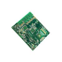
IATF16949 CEM3 Automotive PCB Reverse Engineering High-Tg PCBA Maker Automotive
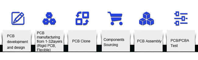
Shenzhen Yideyi Technology Co., Ltd located in Shenzhen . The one of business is PCB reverse research in the begining, but we develop very fast and become the leading enterprice now in the field of reverse technology research. Since establishment, we have been devoting to design, development and reverse technology research of software and hardware products of electronic information industry, and have been a diversified technical service company containing R & D, design and manufacturing.
Core business:
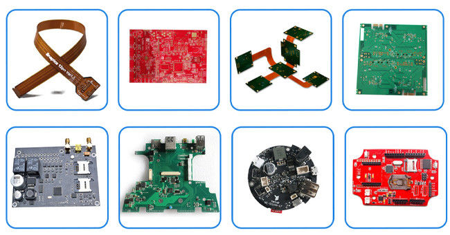
1.PCB copy board/change board(Electronic product clone), PCB backward reasoning/schematic diagram making
2.High-speed PCB design, EMC design, SI simulation analysis
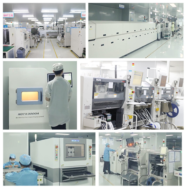
3. SMT/PCBA processing, PCB prototype/batch production
4. Batch component matching procurement, BOM analysis and making
5. Functional prototype manufacturing and test, Difficult component/module substitution
6. Chip decryption and program analysis, IC reverse design, Chip failure analysis, Chip codepoint extraction and copy
7. OEM/ODM of various finished products & semi-finished products
8. Development & solution of large engineering project
Company team:
We attach much importance to cultivate talents and make them full play of their abilities, so now we own the strongest professionally technical team for developing and designing software & hardware, reverse technology research, in which more than 80% technicians with college or above degree. Some technicians of this team are senior engineers, masters, doctors; they have rich practical experience in obverse and reverse research of various electronic products because their researching areas cover computer technology, microelectronics, semiconductor material, mechatronics, industrial automation, etc.
Service idea:
YDY takes "Qualtiy is product's life, credit is company's soul" as business philosophy, "Technology first, market first, credit first, service first" as business principle, "Create the best information product" as development objective. We adhere to provide customers with top-ranking technical solutions, products and service, provide customers with a full set of technical service and complete technical solution of PCB copy board, PCB design, prototype manufacturing, chip decryption, SMT processing and other projects with the best technology and price..
Customer group:
The products YDY research by reverse technology cover industrial, commercial, consumption and military facility fields
How PCB Reverse Engineering Would Help PCB Design & Development?
PCB reverse engineering is a reverse research technology that uses a series of reverse research techniques to obtain a PCB design, circuit schematic and a BOM for an existing & matual electronic design. A new product development that used to take two or three years to develop, now through reverse engineering technolgy, may take only a few months to complete.
In the past decade, the development of electronic technology has been changing with each passing day, and many electronic products have been upgraded at least once a year. Future electronic product updates may be faster. Many electronics engineers have felt that simply using conventional R&D methods can no longer meet the fast steps of modern electronic product replacement, and since there have been millions of matual design in the market, reverse engineering becomes an approach to fast adopt the market pace and catch up the top runners.
YDY service:
1. PCBA, PCB assembly: SMT & PTH & BGA
2. PCBA and enclosure design
3. Components sourcing and purchasing
4. Quick prototyping
5. Plastic injection molding
6. Metal sheet stamping
7. Final assembly
8. Test: AOI, In-Circuit Test (ICT), Functional Test (FCT)
9. Custom clearance for material importing and product exporting
10. PCBA reverse engineering
11. Professtional R&D team
12. PCB Layout Design
Files Requested For Quote:
In order to provide you with the most efficient and accurate quote on manufacturing the requested unit, we ask that you provide us with the following information:
1. Gerber file,PCB file,Eagle file or CAD file are all acceptable
2. A detailed bill of materials (BOM)
3. Clear pictures of PCB or PCBA sample for us
4. Quantity and delivery required
5. Test method for PCBA to guarantee 100% good quality products.
6. Schematics file for PCB design if need to do function test.
7. A sample if available for better sourcing
8. CAD files for enclosure manufacturing if required
9. A complete wiring and assembly drawing showing any special assembly instructions if required
PCB Assembly Manufacturing Procedures:
Program Management
PCB Files → DCC → Program Organizing → Optimization → Checking
SMT Management
PCB Loader → Screen Printer → Checking → SMD Placement → Checking → Air Reflow → Vision Inspection → AOI → Keeping
PCBA Management
THT→Soldering Wave (Manual Welding) → Vision Inspection → ICT → Flash → FCT → Checking → Package → Shipment
Each board is carefully examined by our dedicated inspection team using AOI and high magnification viewers.
Using our X-Ray machine, we test PCBs to component level and all wiring is fully inspected and tested. Flash
testing and earth bonding tests can also be undertaken where required
Why Choose Us?
1. High quality and quick service is our long-term target for customer.
We are strictly control the product quality and provide customers good and quick service, your inquiry related to our products or prices will be replied within 24 hours.
2. Well-trained and experienced salesman or engineering can answer all your inquires with fluent English.
3. Provide OEM&ODM service, we can help you to design and put into product.
4. Protection of your sales area, copyright, ideas of design and all your private information,keep customers information confidential is our responsibility.
5. Reasonable price and top quality products, lower delivery cost help customers cost down and make customers more competitive in the market.
PCBA SMT Manufacture Capacity
| No. | Test item | Criterion | |
| 1 | Voltage: | Charging voltage: | CC/CV: Li-ion/Li-polymer(4.2V/cell); LiFePO4(3.6V/cell) |
| Balance voltage for single cell | Li-ion:4.20 V±0.025V,LiFePO4:3.60V±0.025V | ||
| 2 | Current | Balance current for single cell | 0-125mA |
| Balance current for single cell | ≤20μA | ||
| Maximal continuous charging and discharging current | Charge:20A,Discharge:50A | ||
| 3 | Over-charge Protection | Over charge detection voltage | 3.8-4.4V(can adjust) |
| Over charge detection delay time | 0.5-2.5S | ||
| Over charge release voltage | 3.8-4.4V(can adjust) | ||
| 4 | Over-discharge Protection | Over discharge detection voltage | 1.9-3.1V(can adjust) |
| Over discharge detection delay time | 50-300mS | ||
| Over discharge release voltage | 1.9-3.1V(can adjust) | ||
| 5 | Over-Current Protection | Over current detection voltage | 0.6V |
| Over current detection current | 100-500A | ||
| Detection delay time | 1-50ms | ||
| Release condition | Cut load | ||
| 6 | Short Protection | Detection condition | Exterior short circuit |
| Detection delay time | 200-500us | ||
| Release condition | Cut load | ||
| 7 | Resistance | Protection circuitry(B- to P-) | ≤20mΩ |
| 8 | Temperature | Operating temperature range | -40 to +85degree |
| Storage temperature range | -40 to +125degree | ||
| 9 | Size | L180*W75*T40mm | |
High quality and on-time delivery is always our promise:
FAQ:
Q1. How to keep our product information and design file secret ?
We are willing to sign a NDA effect by customers side local law and
promising to keep customers data in high confidential level.
Q2. How long does it take for PCB and PCBA Quote ?
PCBs quotation within 2 hours can finished the PCBA depend on the
components
quantity,if simple, within 6 hours can finished,once complex and
more,the 12- 36 hours
can be finished.
Q3. Please note that the following detail will speed up evaluation:
Material:
Board thickness:
Copper thickness:Surface finish:
Solder mask color:
Silkscreen color:
Q4. How to make sure the PCBAs are completely well recieved?
We will pack with aluminum bag, and insert card, up and bottom card
with stable cartons.
Q5. How to ship the PCBAs?
For small packages, we will ship the boards to you by
DHL,UPS,FEDEX,TNT. Door to door service! For mass production, we
could ship by air, by sea.
Q6. How to make sure the function is fine?
We could make sample/prototype and do functional testing before
mass production.


