
|
|
[China]

Trade Verify
Address: Room 502, 26# Building, Funing Hi-Tech Industrial Park, Fuhai Street, Bao'an, Shenzhen, Guangdong, China, 518103
Contact name:Helen Jiang

ShenZhen KaiZhuo Electronic Technology Co.,Ltd |
|
Verified Suppliers
|
|
|
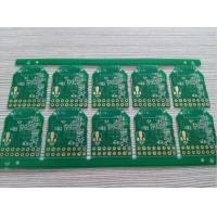
OEM Mobile phone Blue Soldermask White Silkscreen FR4 Electronic Printed Circuit Board
Detail specification about Mobilephone Blue Soldermask White Silkscreen FR4 Electronic Printed Circuit Board
| Categary | PCB |
| Layers | 2L |
| Material | FR-4 |
| Copper thickness | 1/1OZ |
| Board thickness | 1.6mm |
| Soldermask | Blue |
| Quality standard | IPC Class 2, 100% E-testing |
| Certificates | TS16949, ISO9001, UL, RoHS |
Brief introduction about Shenzhen KAZ Circuit Co,. Ltd.
Brief introduction
Shenzhen KAZ Circuit Co., Ltd, found in 2007, is a PCB and PCBA custom-made manufacturer. It's commitment to high precision single, double-sided, multilayer printed circuit board and metal substrate circuit board production,which is a hightech enterprises including amnufacture, sales, service and so on.
We are confident to provide you quality products with factory-directed price within the fastest delivery time!
What KAZ Circuit can do for you:
To get a full quotation of the PCB/PCBA, pls provide the
information as below:
Company Informaiton:
KAZ Circuit is a professional PCB manufacturer from
China since 2007, also provide PCB Assembly service for our
customers. Now with about 300 employees. Certified with
ISO9001,TS16949, UL, RoHS. We are confident to provide you quality
products with factory-directed price within the fastest delivery
time!
Manufacturer Capacity:
| Capacity | Double Sided: 12000 sq.m / month Multilayers: 8000sq.m / month |
| Min Line Width/Gap | 4/4 mil (1mil=0.0254mm) |
| Board Thickness | 0.3~4.0mm |
| Layers | 1~20 layers |
| Material | FR-4, Aluminum, PI |
| Copper Thickness | 0.5~4oz |
| Material Tg | Tg140~Tg170 |
| Max PCB Size | 600*1200mm |
| Min Hole Size | 0.2mm (+/- 0.025) |
| Surface Treatment | HASL, ENIG, OSP |
Electronic printed circuit board (PCB) manufacturing processes:
PCB material choice:
Common base materials include FR-4 (fiberglass),
polyimide and ceramics
Consider properties such as dielectric constant,
thermal performance, and flexibility
Special materials available for high-frequency,
high-power or flexible PCBs
Copper thickness and layer count:
Typical copper foil thickness ranges from 1oz to 4oz
(35µm to 140µm)
Single-sided, double-sided and multilayer PCBs
available
Additional copper layers improve power distribution,
heat dissipation and signal integrity
Surface Treatment:
HASL (Hot Air Solder Leveling) - Affordable, but
surface may not be flat
ENIG (Electroless Nickel Immersion Gold) – provides
excellent solderability and corrosion resistance
Immersion Silver - Cost effective for lead-free
soldering
Additional options include ENEPIG, OSP and direct
gold plating
Advanced PCB Technologies:
Blind and Buried Vias for High Density Interconnects
Microvia Technology for Ultra-Fine Pitch and
Miniaturization
Rigid-flex PCBs for applications that require
flexibility
High frequencies and high speeds with controlled
impedance pc
PCB manufacturing technology:
Subtractive process (most common) - etching away
unwanted copper
Additive process - creating copper traces on the base
material
Semi-additive process - combining subtractive and
additive technologies
Design for Manufacturer (DFM):
Adherence to PCB design guidelines for reliable
manufacturing
Considerations include trace width/spacing, via size
and component location
Close collaboration between designers and
manufacturers is essential
QA and testing:
Electrical testing (e.g., online testing, functional
testing)
Mechanical testing (e.g., bending, shock, vibration)
Environmental testing (e.g., temperature, humidity,
thermal cycles)
More photos


