Active Member
|
[China]

Address: 4/F XingYuan Technology Park,Gushu Tongda Road ,Xixiang Town,Baoan District,Shenzhen,China,518102
Contact name:Victor Zhang

Shenzhen Leadsintec Technology Co., Ltd |
|
|
OEM Custom Prototype PCB Assembly 6 Layers 4.0mm Thickness Through Hole
Prototype PCB Assembly Professional Custom Factory Prototype Service
Thanks for visiting Leadsintec Co., Ltd
We were found a team with more than 20 years in the field. We owns abundant experiences for serving overseas customers from industrial automatic control, communication, medical, Auto and aviation & aerospace,etc. We test our product strictly to guarantee the quality to our customers. We accumulate high reputation during our cooperation.
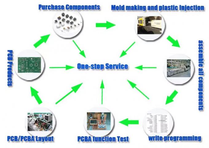
Our Services
1. PCB fabrication.
2. One-stop PCBA: PCB+components sourcing+SMD and through-hole
assembly
PCB Technical Specification
| Order Quantity | 1-500,000 |
| Layer | 1,2,4,6,upto 48 layer |
| Material | FR-4,glass epoxy,FR4 High Tg,Rohs compliant,Aluminum,Rogers,etc |
| PCB type | Rigid,flexible,rigid-flexible |
| Shape | Any shape: Rectangular,round,slots,cutouts,complex,irregular |
| Max PCB dimensions | 700mm*500mm |
| Thickness | 0.4~4.0mm |
| Thickness tolerance | ± 10% |
| Copper thickness | 1/2OZ 1OZ 2OZ 3OZ |
| Copper thickness tolerance | ± 0.25oz |
| Surface finish | HASL,Nickle,Imm Gold,Imm Tin,Imm Silver,OSP etc |
| Solder mask | Green, red,white,yellow,blue,black, Double-sided |
| Silk screen | White,yellow,black,or negative, Double-sided or single-sided |
| Silk screen min line width | 0.006'' or 0.15mm |
| Min drill hole diameter | 0.01'',0.25mm.or 10 mil |
| Min trace/gap | 0.075mm or 3mil |
| PCB cutting | Shear,V-score,tab-routed |
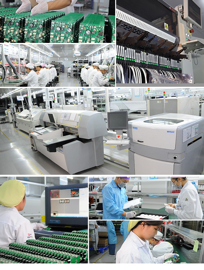
PCB Assembly Capabilities
| One-stop PCBA | PCB+components sourcing+assembly+package |
| Assembly details | SMT and Thru-hole, ISO lines |
| Lead Time | Prototype: 15 work days. Mass order: 20~25 work days |
| Testing on products | Flying Probe Test, X-ray Inspection, AOI Test, functional test |
| Quantity | Min quantity: 1pcs. Prototype, small order, mass order, all OK |
| Files we need | PCB: Gerber files(CAM, PCB, PCBDOC) |
| Components: Bill of Materials(BOM list) | |
| Assembly: Pick-N-Place file | |
| PCB panel Size | Min size: 0.25*0.25 inches(6*6mm) |
| Max size: 20*20 inches(500*500mm) | |
| PCB Solder Type | Water Soluble Solder Paste, RoHS lead free |
| Components details | Passive Down to 0201 size |
| BGA and VFBGA | |
| Leadless Chip Carriers/CSP | |
| Double-sided SMT Assembly | |
| Fine Pitch to 0.8mils | |
| BGA Repair and Reball | |
| Part Removal and Replacement | |
| Component package | Cut Tape,Tube,Reels,Loose Parts |
| PCB assembly process | Drilling-----Exposure-----Plating-----Etaching & Stripping-----Punching-----Electrical Testing-----SMT-----Wave Soldering-----Assembling-----ICT-----Function Testing-----Temperature & Humidity Testing |
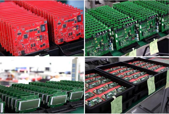
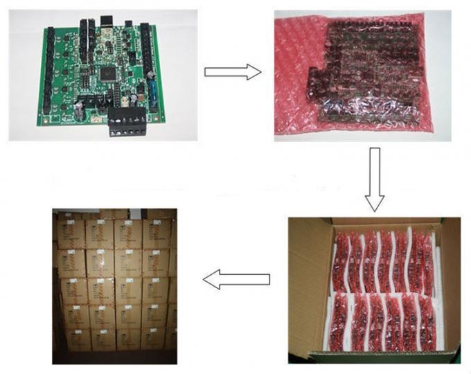
Packing Steps:
PCBAs are packed into Electrostatic bags. Each PCBA foam interval to prevent collision.