
|
|
[China]

Trade Verify
Address: Rm5-616,NO.851,Dianshanhu road; Qingpu area;shanghai city//201799
Contact name:Wang

SHANGHAI FAMOUS TRADE CO.,LTD |
|
Verified Suppliers
|
|
|
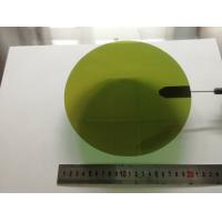
Custom Size Ceramic Substrate / Silicon Carbide Ceramic Excellent CorrosionSingle crystal single side polished silicon wafer sic wafer polishing wafer manufacturer Silicon Carbide SiC Wafer4H-N SIC ingots/High purity 4H-N 4inch 6inch dia 150mm silicon carbide single crystal (sic) substrates wafers, sic crystal ingots sic semiconductor substrates,Silicon Carbide crystal Wafer/ Customzied as-cut sic wafers
Silicon carbide (SiC), also known as carborundum, is a semiconductor containing silicon and carbon with chemical formula SiC. SiC is used in semiconductor electronics devices that operate at high temperatures or high voltages, or both.SiC is also one of the important LED components, it is a popular substrate for growing GaN devices, and it also serves as a heat spreader in high-power LEDs.
| Property | 4H-SiC, Single Crystal | 6H-SiC, Single Crystal |
| Lattice Parameters | a=3.076 Å c=10.053 Å | a=3.073 Å c=15.117 Å |
| Stacking Sequence | ABCB | ABCACB |
| Mohs Hardness | ≈9.2 | ≈9.2 |
| Density | 3.21 g/cm3 | 3.21 g/cm3 |
| Therm. Expansion Coefficient | 4-5×10⁻⁶/K | 4-5×10⁻⁶/K |
| Refraction Index @750nm | no = 2.61 ne = 2.66 | no = 2.60 ne = 2.65 |
| Dielectric Constant | c~9.66 | c~9.66 |
| Thermal Conductivity (N-type, 0.02 ohm.cm) | a~4.2 W/cm·K@298K c~3.7 W/cm·K@298K | |
| Thermal Conductivity (Semi-insulating) | a~4.9 W/cm·K@298K c~3.9 W/cm·K@298K | a~4.6 W/cm·K@298K c~3.2 W/cm·K@298K |
| Band-gap | 3.23 eV | 3.02 eV |
| Break-Down Electrical Field | 3-5×10⁶V/cm | 3-5×10⁶V/cm |
| Saturation Drift Velocity | 2.0×10⁵m/s | 2.0×10⁵m/s |
Physical & Electronic Properties of
Wide Energy Bandgap (eV)
4H-SiC: 3.26 6H-SiC: 3.03 GaAs: 1.43 Si: 1.12
Electronic devices formed in SiC can operate at extremely high temperatures without suffering from intrinsic conduction effects because of the wide energy bandgap. Also, this property allows SiC to emit and detect short wavelength light which makes the fabrication of blue light emitting diodes and nearly solar blind UV photodetectors possible.
High Breakdown Electric Field [V/cm (for 1000 V operation)]
4H-SiC: 2.2 x 106* 6H-SiC: 2.4 x 10⁶* GaAs: 3 x 10⁵ Si: 2.5 x 10⁵
SiC can withstand a voltage gradient (or electric field) over eight times greater than than Si or GaAs without undergoing avalanche breakdown. This high breakdown electric field enables the fabrication of very high-voltage, high-power devices such as diodes, power transitors, power thyristors and surge suppressors, as well as high power microwave devices. Additionally, it allows the devices to be placed very close together, providing high device packing density for integrated circuits.
High Thermal Conductivity (W/cm · K @ RT)
4H-SiC: 3.0-3.8 6H-SiC: 3.0-3.8 GaAs: 0.5 Si: 1.5
SiC is an excellent thermal conductor. Heat will flow more readily through SiC than other semiconductor materials. In fact, at room temperature, SiC has a higher thermal conductivity than any metal. This property enables SiC devices to operate at extremely high power levels and still dissipate the large amounts of excess heat generated.
High Saturated Electron Drift Velocity [cm/sec (@ E ≥ 2 x 10⁵ V/cm)]
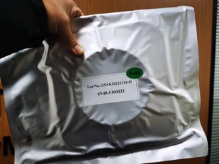
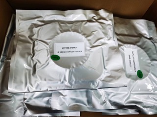
Product show:
4H-SiC: 2.0 x 10⁷ 6H-SiC: 2.0 x 10⁷ GaAs: 1.0 x 10⁷ Si: 1.0 x 10⁷
SiC devices can operate at high frequencies (RF and microwave)
because of the high saturated electron drift velocity of SiC.


About ZMKJ Company
ZMKJ can provides high quality single crystal SiC wafer ( Silicon Carbide ) to electronic and optoelectronic industry . SiC wafer is a next generation semiconductor material , with unique electrical properties and excellent thermal properties , compared to silicon wafer and GaAs wafer , SiC wafer is more suitable for high temperature and high power device application . SiC wafer can be supplied in diameter 2-6 inch , both 4H and 6H SiC , N-type , Nitrogen doped , and semi-insulating type available . Please contact us for more product information .
FAQ:
Q: What's the way of shipping and cost?
A:(1) We accept DHL, Fedex, EMS etc.
(2) it is fine If you have your own express account ,If not,we could help you ship them and
Freight is in accordance with the actual settlement.
Q: How to pay?
A: T/T 100% deposit before delivery.
Q: What's your MOQ?
A: (1) For inventory, the MOQ is 1pcs. if 2-5pcs it's better.
(2) For customized commen products, the MOQ is 10pcs up.
Q: What's the delivery time?
A: (1) For the standard products
For inventory: the delivery is 5 workdays after you place the order.
For customized products: the delivery is 2 -4 weeks after you order contact.
Q: Do you have standard products?
A: Our standard products in stock. as like substrates 4inch 0.35mm.


