
|
|
[China]

Trade Verify
Address: Rm5-616,NO.851,Dianshanhu road; Qingpu area;shanghai city//201799
Contact name:Wang

SHANGHAI FAMOUS TRADE CO.,LTD |
|
Verified Suppliers
|
|
|
2inch/3inch/4inch/6inch 6H-N/4H-SEMI/ 4H-N SIC ingots/High purity 4H-N 4inch 6inch dia 150mm silicon carbide single crystal (sic) substrates wafers,
40x3mmt customized shape 6H-semi type sic wafers silicon carbon chips for optical
Silicon carbide (SiC), also known as carborundum, is a semiconductor containing silicon and carbon with chemical formula SiC. SiC is used in semiconductor electronics devices that operate at high temperatures or high voltages, or both.SiC is also one of the important LED components, it is a popular substrate for growing GaN devices, and it also serves as a heat spreader in high-power LEDs.
Application of SiC in power device industry
Compared with silicon devices, silicon carbide (SiC) power devices can effectively achieve high efficiency, miniaturization and light weight of power electronic systems. The energy loss of SiC power devices is only 50% of Si devices, and the heat generation is only 50% of silicon devices, SiC also has a higher current density. At the same power level, the volume of SiC power modules is significantly smaller than that of silicon power modules. Taking the intelligent power module IPM as an example, using SiC power devices, the module volume can be reduced to 1/3 to 2/3 of silicon power modules.
There are three types of SiC power diodes: Schottky diodes (SBD), PIN diodes and junction barrier controlled Schottky diodes (JBS). Because of the Schottky barrier, SBD has a lower junction barrier height, so SBD has the advantage of low forward voltage. The emergence of SiC SBD has enlarged the application range of SBD from 250V to 1200V. In addition, its characteristics at high temperature are good, the reverse leakage current not increases from room temperature to 175 ° C. In the application field of rectifiers above 3kV, SiC PiN and SiC JBS diodes have received much attention due to their higher breakdown voltage, faster switching speed, smaller size and lighter weight than silicon rectifiers.
SiC power MOSFET devices have ideal gate resistance, high-speed switching performance, low on-resistance, and high stability. It is the preferred device in the field of power devices below 300V. There are reports that a silicon carbide MOSFET with a blocking voltage of 10kV has been successfully developed. Researchers believe that SiC MOSFETs will occupy an advantageous position in the field of 3kV - 5kV.
SiC Insulated Gate Bipolar Transistors (SiC BJT, SiC IGBT) and SiC Thyristor (SiC Thyristor), SiC P-type IGBT devices with a blocking voltage of 12 kV have good forward current capability. Compared with Si bipolar transistors, SiC bipolar transistors have 20-50 times lower switching losses and lower turn-on voltage drop. SiC BJT is mainly divided into epitaxial emitter BJT and ion implantation emitter BJT, the typical current gain is between 10-50.
| Properties | unit | Silicon | SiC | GaN |
| Bandgap width | eV | 1.12 | 3.26 | 3.41 |
| Breakdown field | MV/cm | 0.23 | 2.2 | 3.3 |
| Electron mobility | cm^2/Vs | 1400 | 950 | 1500 |
| Drift valocity | 10^7 cm/s | 1 | 2.7 | 2.5 |
| Thermal conductivity | W/cmK | 1.5 | 3.8 | 1.3 |
Application of SiC in LED industry
At present, the sapphire crystal is the first choice for the substrate material used in the optoelectronic device industry, but sapphire has some shortcomings that cannot be overcome, such as lattice mismatch, thermal stress mismatch, high resistivity as an insulator, and poor thermal conductivity. Therefore, the excellent characteristics of SiC substrates have attracted much attention and are more suitable as substrate materials for gallium nitride (GaN) -based light-emitting diodes (LEDs) and laser diodes (LDs). Data from Cree shows that the use of silicon carbide The substrate LED device can achieve a 70% light maintenance rate life of up to 50,000 hours. The advantages of SiC as LED substrate:
* The lattice constant of SiC and GaN epitaxial layer are matched, and the chemical characteristics are compatible;
* SiC has excellent thermal conductivity (more than 10 times higher than sapphire) and close to the thermal expansion coefficient of GaN epitaxial layer;
* SiC is a conductive semiconductor, which can be used to make vertical structure devices. Two electrodes are distributed on the surface and bottom of the device, it can solve the various shortcomings caused by the horizontal structure of sapphire substrate;
* SiC does not require a current diffusion layer, light will not be absorbed by the material of the current diffusion layer, which improves the light extraction efficiency.
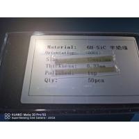
Silicon Carbide (SiC) Substrate Specification
Silicon Carbide SiC crystal substrate wafer carborundum
The specification of 3'' Inch
| Grade | Production | Research Grade | Dummy Grade | |
| Diameter | 50.8 mm±0.38 mm or other size | |||
| Thickness | 330 μm±25μm | |||
| Wafer Orientation | On axis: <0001>±0.5° for 6H-N/4H-N/4H-SI/6H-SI Off axis : 4.0° toward1120 ±0.5° for 4H-N/4H-SI | |||
| Micropipe Density | ≤5 cm-2 | ≤15 cm-2 | ≤50 cm-2 | |
| Resistivity | 4H-N | 0.015~0.028 Ω·cm | ||
| 6H-N | 0.02~0.1 Ω·cm | |||
| 4/6H-SI | >1E5 Ω·cm | (90%) >1E5 Ω·cm | ||
| Primary Flat | {10-10}±5.0° | |||
| Primary Flat Length | 22.2 mm±3.2 mm | |||
| Secondary Flat Length | 11.2mm±1.5 mm | |||
| Secondary Flat Orientation | Silicon face up: 90° CW. from Prime flat ±5.0° | |||
| Edge exclusion | 2 mm | |||
| TTV/Bow /Warp | ≤15μm /≤25μm /≤25μm | |||
| Roughness | Polish Ra≤1 nm | |||
| CMP Ra≤0.5 nm | ||||
| Cracks by high intensity light | None | 1 allowed, ≤ 1mm | 1 allowed, ≤2 mm | |
| Hex Plates by high intensity light | Cumulative area≤1 % | Cumulative area≤1 % | Cumulative area≤3 % | |
| Polytype Areas by high intensity light | None | Cumulative area≤2 % | Cumulative area≤5 % | |
| Scratches by high intensity light | 3 scratches to 1×wafer diameter cumulative length | 5 scratches to 1×wafer diameter cumulative length | 8 scratches to 1×wafer diameter cumulative length | |
| Edge chip | None | 3 allowed, ≤0.5 mm each | 5 allowed, ≤1 mm each | |
| Contamination by high intensity light | None | |||


About ZMKJ Company
ZMKJ can provides high quality single crystal SiC wafer ( Silicon Carbide ) to electronic and optoelectronic industry . SiC wafer is a next generation semiconductor material , with unique electrical properties and excellent thermal properties , compared to silicon wafer and GaAs wafer , SiC wafer is more suitable for high temperature and high power device application . SiC wafer can be supplied in diameter 2-6 inch , both 4H and 6H SiC , N-type , Nitrogen doped , and semi-insulating type available . Please contact us for more product information .
FAQ:
Q: What's the way of shipping and cost?
A:(1) We accept DHL, Fedex, EMS etc.
(2) it is fine If you have your own express account ,If not,we could help you ship them and
Freight is in accordance with the actual settlement.
Q: How to pay?
A: T/T 100% deposit before delivery.
Q: What's your MOQ?
A: (1) For inventory, the MOQ is 1pcs. if 2-5pcs it's better.
(2) For customized commen products, the MOQ is 10pcs up.
Q: What's the delivery time?
A: (1) For the standard products
For inventory: the delivery is 5 workdays after you place the order.
For customized products: the delivery is 2 -4 weeks after you order contact.
Q: Do you have standard products?
A: Our standard products in stock. as like substrates 4inch 0.35mm.


