|
|
[China]

Trade Verify
Address: Rm5-616,NO.851,Dianshanhu road; Qingpu area;shanghai city//201799
Contact name:Wang

SHANGHAI FAMOUS TRADE CO.,LTD |
|
Verified Suppliers
|
|
|
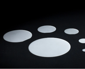
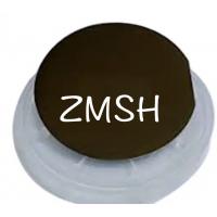
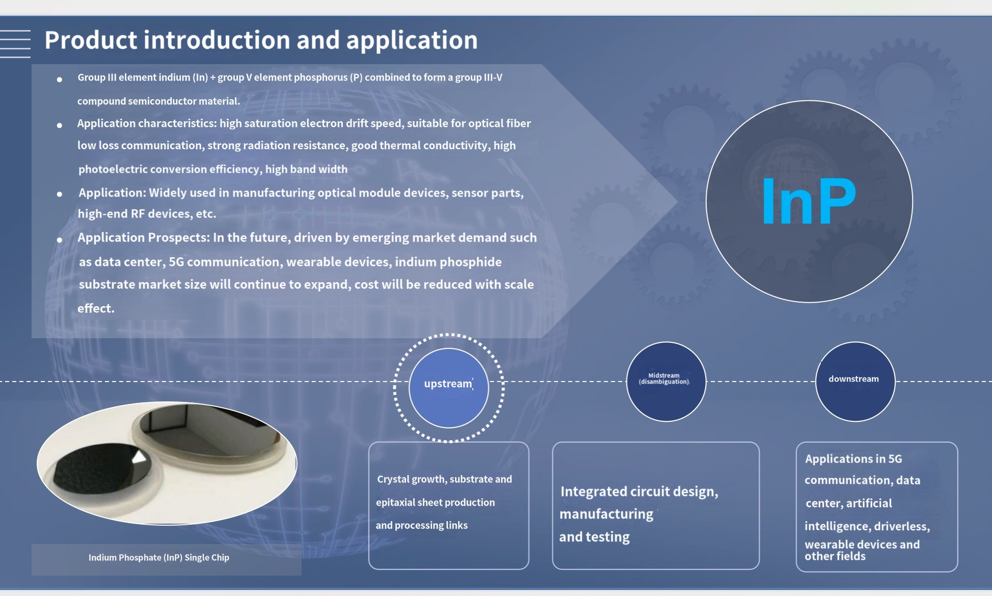
Epi ready 4inch InP wafers N-type p-type EPF<1000cm^2 with the thickness of 325um±50um

Our product, the "High-Purity Indium Phosphide (InP) Wafer," stands at the forefront of semiconductor innovation. Crafted from pristine indium phosphide, a binary semiconductor renowned for its superior electron velocity, our wafer offers unparalleled performance in optoelectronic applications, rapid transistors, and resonance tunneling diodes. With widespread utility in high-frequency and high-power electronic devices, our wafer is a cornerstone of next-gen technology. Its proficiency in high-speed fiber optic communication, enabled by its ability to emit and detect wavelengths above 1000nm, further solidifies its importance in modern telecommunications. Serving as a substrate for laser and photodiodes in Datacom and Telecom applications, our wafer seamlessly integrates into critical infrastructures. As the era of 5G approaches, our product emerges as a cornerstone, facilitating optical fiber connections, metro-ring access networks, and data centers worldwide. Offering 99.99% purity, our indium phosphide wafers ensure unmatched efficiency and effectiveness, propelling technological advancement into the future.
Superior Electron Velocity: Derived from indium phosphide, our wafers boast exceptional electron velocity, surpassing that of conventional semiconductors like silicon. This attribute underpins their efficacy in optoelectronic applications, rapid transistors, and resonance tunneling diodes.
High-Frequency Performance: Our wafers find widespread use in high-frequency and high-power electronic devices, demonstrating their capability to support demanding operational requirements with ease.
Optical Efficiency: With a capacity to emit and detect wavelengths above 1000nm, our wafers excel in high-speed fiber optic communication systems, ensuring reliable data transmission across diverse networks.
Versatile Substrate: Serving as a substrate for laser and photodiodes in Datacom and Telecom applications, our wafers seamlessly integrate into various technological infrastructures, facilitating robust performance and scalability.
Purity and Reliability: Offering 99.99% purity, our indium phosphide wafers guarantee consistent performance and durability, meeting the stringent demands of modern telecommunications and data technologies.
Future-Proof Design: Positioned at the forefront of semiconductor innovation, our wafers anticipate the needs of emerging technologies, making them indispensable components for optical fiber connections, metro-ring access networks, and data centers amidst the impending 5G revolution.
Specifications:
| Material | InP single crystal | Orientation | <100> |
| Size(mm) | Dia50.8×0.35mm,10×10×0.35mm 10×5×0.35mm | Surface Roughness | Ra:≤5A |
| Polishing | SSP (single surface polished) or DSP (double surface polished) | ||
Chemical Properties of InP Crystal:
| Single Crystal | Doped | Conduction Type | Carrier Concentration | Mobility Ratio | Dislocation Density | Standard Size |
| InP | / | N | (0.4-2)×1016 | (3.5-4) ×103 | 5×10⁴ | Φ2"×0.35mm Φ3"×0.35mm |
| InP | S | N | (0.8-3) ×1018 (4-6) ×1018 | (2.0-2.4) ×103 (1.3-1.6) ×103 | 3×10⁴ 2×10³ | Φ2"×0.35mm Φ3"×0.35mm |
| InP | Zn | P | (0.6-2) ×1018 | 70-90 | 2×10⁴ | Φ2"×0.35mm Φ3"×0.35mm |
| InP | Fe | N | 107-108 | ≥2000 | 3×10⁴ | Φ2"×0.35mm Φ3"×0.35mm |
Basic Properties:
| Crystal Structure | Tetrahedral(M4) | Lattice Constant | a = 5.869 Å |
| Density | 4.81g/cm3 | Melt Point | 1062 °C |
| Molar Mass | 145.792 g/mol | Appearance | Black cubic crystals |
| Chemical Stability | Slightly soluble in acids | Electron Mobility(@300K) | 5400 cm2/(V·s) |
| Bandgap(@300 K) | 1.344eV | Thermal Conductivity(@300K) | 0.68 W/(cm·K) |
| Refractive Index | 3.55(@632.8nm) | ||
Optoelectronic Devices: Our indium phosphide wafers are extensively used in optoelectronic applications, including light-emitting diodes (LEDs), laser diodes, and photodetectors. Their superior electron velocity and optical efficiency make them ideal for producing high-performance optoelectronic components.
High-Speed Transistors: The exceptional electron velocity of our wafers enables the fabrication of high-speed transistors, essential for applications requiring rapid signal processing and switching speeds. These transistors find use in telecommunications, computing, and radar systems.
Fiber Optic Communication: Indium phosphide wafers are indispensable in high-speed fiber optic communication systems due to their ability to emit and detect wavelengths above 1000nm. They enable the transmission of data over long distances with minimal signal loss, making them vital for telecommunications networks and data centers.
Resonance Tunneling Diodes: Our wafers are utilized in the production of resonance tunneling diodes, which exhibit unique quantum tunneling effects. These diodes find applications in high-frequency oscillators, terahertz imaging, and quantum computing.
High-Frequency Electronics: InP wafers are commonly employed in high-frequency and high-power electronic devices, including microwave amplifiers, radar systems, and satellite communications. Their high electron mobility and reliability make them suitable for demanding aerospace and defense applications.
Datacom and Telecom Infrastructure: Serving as substrates for laser diodes and photodiodes, our wafers contribute to the development of Datacom and Telecom infrastructure, supporting high-speed data transmission and telecommunications networks. They are integral components in optical transceivers, fiber optic switches, and wavelength division multiplexing systems.
Emerging Technologies: As emerging technologies such as 5G, Internet of Things (IoT), and autonomous vehicles continue to evolve, the demand for indium phosphide wafers will only increase. These wafers will play a crucial role in enabling the next generation of wireless communication, sensor networks, and smart devices.