
|
|
[China]

Trade Verify
Address: Rm5-616,NO.851,Dianshanhu road; Qingpu area;shanghai city//201799
Contact name:Wang

SHANGHAI FAMOUS TRADE CO.,LTD |
|
Verified Suppliers
|
|
|
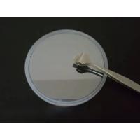
VGF 2 Inch 4Inch N Type P Type GaAs Wafer Semiconductor Substrate For Epitaxial Growth
Gallium arsenide can be made into semi-insulating high-resistance materials with resistivity more than 3 orders of magnitude higher than silicon and germanium, which are used to make integrated circuit substrates, infrared detectors, gamma photon detectors, etc. Because its electron mobility is 5 to 6 times greater than that of silicon, it has important applications in the manufacture of microwave devices and high-speed digital circuits. Gallium arsenide made of gallium arsenide can be made into semi-insulating high-resistance materials with resistivity of more than 3 orders of magnitude higher than silicon and germanium, which are used to make integrated circuit substrates and infrared detectors.
1. Application of gallium arsenide in optoelectronics
2. Application of gallium arsenide in microelectronics
3. Application of gallium arsenide in communication
4. Application of gallium arsenide in microwave
5. Application of gallium arsenide in solar cells
| Type/Dopant | Semi-Insulated | P-Type/Zn | N-Type/Si | N-Type/Si |
| Application | Micro Eletronic | LED | Laser Diode | |
| Growth Method | VGF | |||
| Diameter | 2", 3", 4", 6" | |||
| Orientation | (100)±0.5° | |||
| Thickness (µm) | 350-625um±25um | |||
| OF/IF | US EJ or Notch | |||
| Carrier Concentration | - | (0.5-5)*1019 | (0.4-4)*1018 | (0.4-0.25)*1018 |
| Resistivity (ohm-cm) | >107 | (1.2-9.9)*10-3 | (1.2-9.9)*10-3 | (1.2-9.9)*10-3 |
| Mobility (cm2/V.S.) | >4000 | 50-120 | >1000 | >1500 |
| Etch Pitch Density (/cm2) | <5000 | <5000 | <5000 | <500 |
| TTV [P/P] (µm) | <5 | |||
| TTV [P/E] (µm) | <10 | |||
| Warp (µm) | <10 | |||
| Surface Finished | P/P, P/E, E/E | |||
Gallium arsenide is the most important and widely used semiconductor material in compound semiconductors, and it is also the most mature and the largest compound semiconductor material in production at present.


