
|
|
[China]

Trade Verify
Address: Rm5-616,NO.851,Dianshanhu road; Qingpu area;shanghai city//201799
Contact name:Wang

SHANGHAI FAMOUS TRADE CO.,LTD |
|
Verified Suppliers
|
|
|
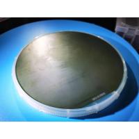
2inch 4/6inch dia200mm sic seed wafer 1mm thickness for ingot growth High Purity 4 6 8-inch conductive semi-insulation SiC single crystal wafer
Customized size/2inch/3inch/4inch/6inch 6H-N/4H-SEMI/ 4H-N SIC ingots/High purity 4H-N 4inch 6inch dia 150mm silicon carbide single crystal (sic) substrates wafers/ Customzied as-cut sic wafers production 4inch grade 4H-N 1.5mm SIC Wafers for seed crystal 4inch 6inch seed sic wafer 1.0mm Thickness 4h-N SIC Silicon Carbide Wafer For seed growth
Product Name | SIC |
Polytype | 4H |
Surface orientation on-axis | 0001 |
Surface orientation off-axis | 0± 0.2° |
FWHM | ≤45arcsec |
Type | HPSI |
Resistivity | ≥1E9ohm·cm |
Diameter | 99.5~100mm |
Thickness | 500±25μm |
Primary flat orientation | [1-100]± 5° |
Primary flat length | 32.5± 1.5mm |
Secondary flat position | 90° CW from primary flat ± 5°, silicon face up |
Secondary flat length | 18± 1.5mm |
TTV | ≤5μm |
LTV | ≤2μm(5mm*5mm) |
Bow | -15μm~15μm |
Warp | ≤20μm |
(AFM) Front (Si-face) Roughn | Ra≤0.2nm(5μm*5μm) |
Micropipe Density | ≤1ea/cm2 |
Carbon Density | ≤1ea/cm2 |
Hexagonal void | None |
Metal impurities | ≤5E12atoms/cm2 |
Front | Si |
Surface Finish | CMP Si-face CMP |
Particles | size≥0.3μm) |
Scratches | ≤Diameter (Cumulative Length) |
Orange peel/pits/stains/striations/cracks/contaminati on | None |
Edge chips/indents/fracture/hex plates | None |
Polytype areas | None |
Front laser marking | None |
Back Finish | C-face CMP |
Scratches | ≤2*Diameter (Cumulative Length) |
Back defects (edge chips/indents) | None |
Back roughness | Ra≤0.2nm(5μm*5μm) |
Back laser marking | 1mm (from top edge) |
Edge | Chamfer |
Packaging | The inner bag is filled with nitrogen and the outer bag is
vacuumed. |
Packaging | Multi-wafer cassette, epi-ready. |
SiC single crystal has many excellent properties, such as high thermal conductivity, high saturated electron mobility, strong voltage breakdown resistance, etc., suitable for the preparation of high frequency, high power, high temperature, and radiation-resistant electronic devices.
1--Silicon carbide wafer is mainly used in the production of
SCHOttky diode, metal oxide semiconductor field effect transistor,
junction field effect transistor, bipolar junction transistor,
thyristor, turn-off thyristor and insulated gate bipolar
transistor.
2--SiC power MOSFET devices have ideal gate resistance, high-speed switching performance, low on-resistance, and high stability. It is the preferred device in the field of power devices below 300V. There are reports that a silicon carbide MOSFET with a blocking voltage of 10kV has been successfully developed. Researchers believe that SiC MOSFETs will occupy an advantageous position in the field of 3kV - 5kV.
3--SiC power MOSFET devices have ideal gate resistance, high-speed switching performance, low on-resistance, and high stability. It is the preferred device in the field of power devices below 300V. There are reports that a silicon carbide MOSFET with a blocking voltage of 10kV has been successfully developed. Researchers believe that SiC MOSFETs will occupy an advantageous position in the field of 3kV - 5kV.
Product Display


4H-N Type / High Purity SiC wafer/ingots 2 inch 4H N-Type SiC wafer/ingots 3 inch 4H N-Type SiC wafer 4 inch 4H N-Type SiC wafer/ingots 6 inch 4H N-Type SiC wafer/ingots | 4H Semi-insulating / High Purity SiC wafer 2 inch 4H Semi-insulating SiC wafer 3 inch 4H Semi-insulating SiC wafer 4 inch 4H Semi-insulating SiC wafer 6 inch 4H Semi-insulating SiC wafer |
6H N-Type SiC wafer 2 inch 6H N-Type SiC wafer/ingot | Customized size for 2-6inch |
We specialize in processing a variety of materials into wafers,
substrates, and customized optical glass parts. components widely
used in electronics, optics, optoelectronics, and many other
fields. We also have been working closely with many domestic and
oversea universities, research institutions, and companies, to
provide customized products and services for their R&D
projects.
It's our vision to maintain a good cooperation relationship with
all our customers through our good reputation.
Q: What's the way of shipping and cost?
(1) We accept DHL, Fedex, TNT, UPS, EMS, SF and etc.
(2) If you have your own express account, it's great.
Q: How to pay?
(1) T/T, PayPal, West Union, MoneyGram and
Assurance payment on Alibaba and etc.
(2) Bank Fee: West Union≤USD1000.00),
T/T -: over 1000usd ,please by t/t
Q: What's the deliver time?
(1) For inventory: the delivery time is 5 workdays.
(2) The delivery time is 7 to 25 workdays for customized products.
According to the quantity.
Q: Can I customize the products based on my need?
Yes, we can customize the material, specifications, and optical
coating for your optical components based on your needs.


