
|
|
[China]

Trade Verify
Address: 819# SONGWEI ROAD (N.) SONGJIANG INDUSTRIAL ZONE, SHANG HAI, CHINA 201613
Contact name:ZHOU XIN

SHANGHAI ROYAL TECHNOLOGY INC. |
|
Verified Suppliers
|
|
|
Technical Background
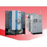
The RTSP1200-PCB machine is a tailor-designed and fabricated
equipment for PCBs plating by magnetron sputtering deposition
technology.
Everyone who is involved with the PCB industry knows that PCBs which have copper finishes on the surface requires a protective layer to protect it against from oxidize and deteriorate, meanwhile the film must with high hardness and abrasion resistance to guarantee the lifetime.
Royal Technology spent 6 months in R&D, over 20 times experiment to finalized the proper coating processes. More exciting new is in March 2020, we delivered the massive production machine to our customer’s site with a high accomplishment result.
Key Features
Multiple deposition cathodes for fast deposition rate
Strong vacuum pumping system for a short cycle
Anode linear ion source to improve adhesion and high density of
deposited films
6 units standard planar cathodes mounting flanges
Flexible coating processes applied
Modular structure design for fast exchange of cathodes and targets

Planar Sputtering Cathodes
Technical Specifications
| Description | RTSP1200-PCB |
| Advantages | Environmentally friendly process Much lower production cost compared with conventional metal electroplating process Excellent corrosion and wear resistance Hign density and high uniformity Film thickness can be well controlled |
| Deposited Films | Au gold, Ag silver, Cu copper conductive families films; Corrosion resistance metal families: Tantalum(Ta), Nickle (Ni), Chrome (Cr), Zirconium(Zr) etc. Compounded films: carbon-based metal films, Nitride metal films. |
| Deposition Chamber | Cylinder chamber with vertical orientation, one door structure with front opening method Chammber inner size: φ1200 * H1500mm
|
| Loading Volume (Max.) | Central driving rack system, with Max. φ1000mm *H1100 |
| Deposition Sources | 4 Planar sputtering cathodes + 1 mounting flange for upgrading |
| Sputtering Deposition Power | Max. 30KW |
| Pulsed Bias Power | Max. 30KW |
| Footprint (L*W*H) | 5000*5000*4500mm |
| Power Consumption | Max. 105KW Average:50KW |
| Operation & Control System | CE standard Mitsubishi PLC+ Touch Screen Operation Program with backup |
These configurations are standard, for a specific developing market and new special coatings, the customized configurations and modifications are available on requests.
6-RT1200-PCB- Magnetron sputtering deposition equi... for more details, please download catalogue here.

Operation and Coating Process Training for Customers


