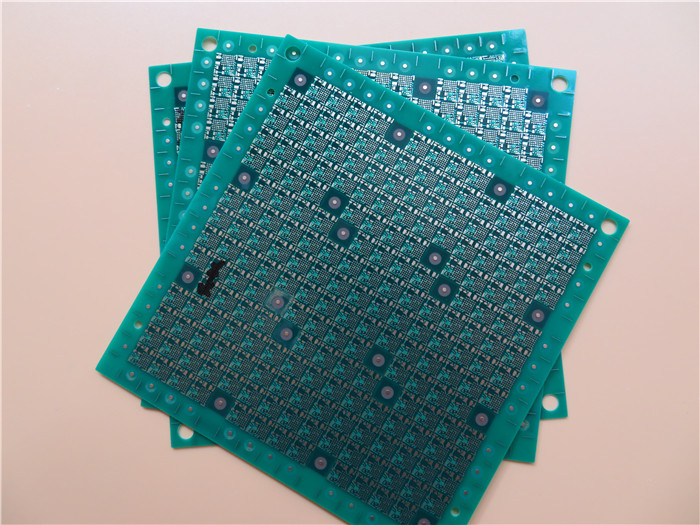
Via Filled PCB Via in Pad Circuit Board 0.6mm Multilayer PCB Built
On 6 Layer With Blind Via for GPS Tracking
1.1 General description
This is a type of 6 layer ultrathin printed circuit board built on
FR-4 substrate with Tg 135°C for the application of GPS Tracking.
It's only 0.6 mm thick without silkscreen on green solder mask
(Taiyo) and immersion gold on pads. The base material is from
Taiwan ITEQ supplying 1 up PCB per panel. Vias with 0.25mm are
resin filled and capped (via in pad). They're fabricated per IPC
6012 Class 2 using supplied Gerber data. Each 50 panels are packed
for shipment.
1.2 Features and benifits
RoHS compliant and suitable for thermal reliability needs
High solderability, no stressing of circuit boards and less
contamination of PCB surface.
Comprehensive equipment management and maintenance and process
control
Products and Manufacturing are certified by authorized
organizations.
Small quantity order is accepted
Delivery on time: >98%
1.3 Applications
Led Lighting
Intercom System
Portable WiFi Router
GSM Tracker
Commercial Led Lighting
Modem WiFi 4G
Honeywell Access Control
Electronic Access Control
Audio Frequency Amplifier
File servers
1.4 Parameter and data sheet
| PCB SIZE | 100 x 103mm=1PCS |
| BOARD TYPE | Multilayer PCB |
| Number of Layers | 6 layers |
| Surface Mount Components | YES |
| Through Hole Components | NO |
| LAYER STACKUP | copper ------- 18um(0.5oz)+plate TOP CS |
| 4mil prepreg |
| copper ------- 18um(0.5oz) GND Plane |
| 4mil FR-4 |
| copper ------- 18um(0.5oz) PWR Plane |
| 4mil prepreg |
| copper ------- 18um(0.5oz) PWR Plane |
| 4mil FR-4 |
| copper ------- 18um(0.5oz) SIG |
| 4mil prepreg |
| copper ------- 18um(0.5oz) BOT PS |
| TECHNOLOGY | |
| Minimum Trace and Space: | 3mil/3mil |
| Minimum / Maximum Holes: | 0.22/3.50mm |
| Number of Different Holes: | 25 |
| Number of Drill Holes: | 2315 |
| Number of Milled Slots: | 0 |
| Number of Internal Cutouts: | 0 |
| Impedance Control | no |
| BOARD MATERIAL | |
| Glass Epoxy: | FR-4, ITEQ IT140 TG>135, er<5.4 |
| Final foil external: | 1oz |
| Final foil internal: | 0.5oz |
| Final height of PCB: | 0.6mm ±0.1 |
| PLATING AND COATING | |
| Surface Finish | Immersion gold 0.025µm over 3µm Nickel (14.4% area) |
| Solder Mask Apply To: | TOP and Bottom, 12micron Minimum |
| Solder Mask Color: | Green, TAIYO PSR-2000 GT600D |
| Solder Mask Type: | LPSM |
| CONTOUR/CUTTING | Routing |
| MARKING | |
| Side of Component Legend | No silkscreen requried. |
| Colour of Component Legend | No silkscreen requried. |
| Manufacturer Name or Logo: | No silkscreen requried. |
| VIA | Plated through hole(PTH), Blind via and via capping on CS and PS,
vias not be visible. |
| FLAMIBILITY RATING | UL 94-V0 Approval MIN. |
| DIMENSION TOLERANCE | |
| Outline dimension: | 0.0059" (0.15mm) |
| Board plating: | 0.0030" (0.076mm) |
| Drill tolerance: | 0.002" (0.05mm) |
| TEST | 100% Electrical Test prior shipment |
| TYPE OF ARTWORK TO BE SUPPLIED | email file, Gerber RS-274-X, PCBDOC etc |
| SERVICE AREA | Worldwide, Globally. |
1.5 Design For Manufacture (2)
| Serial NO. | Procedure | Item | Manufacturing capability |
| Large volume (S<100 m²) | Middle volume (S<10 m²) | Prototype(S<1m²) |
|
| 14 | Laminating | Tolerance of laminate thickness | ±10% PCB thick | ±10% PCB thick | ±8% PCB thick |
| 15 | Maximum laminate thickness | 4.0mm | 6.0mm | 7.0mm |
| 16 | Laminate alignment accuracy | ≤±5 mil | ≤±4 mil | ≤±4 mil |
| 17 | Drill (18um, 35um, 70um etc are finished copper. If not mentioned
copper, finished 1oz is the default value ) | Min.drill bit diameter | 0.2 mm | 0.2 mm | 0.2 mm |
| 18 | Min.slot router diameter | 0.60 mm | 0.60 mm | 0.60 mm |
| 19 | Min.tolerance of PTH slots | ±0.15mm | ±0.15mm | ±0.1mm |
| 20 | Max.aspect ratio | 1:08 | 1:12 | 1:12 |
| 21 | Hole tolerance | ±3mil | ±3mil | ±3mil |
| 22 | Space of via to via | 6mil(same net),12mil(different net) | 6mil(same net),14mil(different net) | 4mil(same net),12mil(different net) |
| 23 | Space of component hole to component hole | 12mil(same net),16mil(different net) | 12mil(same net),16mil(different net) | 10mil(same net),14mil(different net) |
| 24 | Etching | Min.width of etching logo | 10mil(18um),12 mil (35um),12 mil(70um) | 8mil(18um),10mil(35um),12 mil(70um) | 6mil(18um),8 mil(35um),12mil(70um) |
| 25 | Etch factor | 1.6-2.2 | 1.6-2.2 | 1.6-2.2 |
| 26 | Outer layer(18um, 35um, 70um etc are finished copper. If not
mentioned copper, finished 1oz is the default value ) | Min.via pad diameter | 20mil | 16mil | 16mil |
| 27 | Min.BGA pad diameter | 12mil | 12mil | 10mil |
| 28 | Min.track and spacing | 5/5mil(18um) | 4/4mil(18um) | 3/3.5mil(18um) |
| 5/5mil(35um) | 4/4mil(35um) | 3/4mil(35um) |
| 7/9mil(70um) | 6/8mil(70um) | 6/7mil(70um) |
| 9/11mil(105um) | 8/10mil(105um) | 8/9mil(105um) |
| 13/13mil(140um) | 12/12mil(140um) | 12/11mil(140um) |
| 29 | Minimum grid | 10/10mil(35um) | 8/8mil(35um) | 4/8mil(35um) |
| 30 | Min.space (conductor to pad, pad to pad) | 6mil(18um) | 5mil(18um) | 4mil(18um) |
| 6mil(35um) | 5mil(35um) | 4mil(35um) |
| 9mil(70um) | 8mil(70um) | 7mil(70um) |
| 11mil(105um) | 10mil(105um) | 9mil(105um) |
| 13mil(140um) | 12mil(140um) | 11mil(140um) |


