

Active Member
|
[China]

Address: Room 1520, Block 11, International E-Commerce Logistics Center, PingAn Road, PingHu Street, LongGang District, ShenZhen City, China 518111
Contact name:Steven YU

Witgain Technology Limited |
|
|
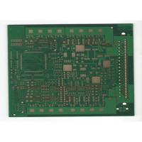
HDI PCB 10 Layer 1.6 MM Thickness FR4 TG170 Material
PCB Specifications:
1 Part NO: HDIPCB0009
2 Layer Count: 10 Layer HDI PCB
3 Finished Board Thickness: 1.6MM
4 Drilling: L1-L2 0.1MM, L3-L8 0.2MM, L9-L10 0.1MM, L1-L10 0.2MM
5 Min Lind Space&Width: 4/6mil
6 Copper Thickness: 1/H/H/H/H/H/H/H/H/1
7 Application Area: Automobiles
Our production applications:
1 Consumer electronic products: SSD, TWS earphones, headsets,computer devices, portable power supplies, bluetooth modules, gps modules, wifi modules, smart keys for cars, intelligent locks, floor mopping robots, zigbee, etc.
2 Industrial control:main boards in machines, industrial robots, servo motors etc.
3 Automotive: BMS main boards, automotive radar etc.
4 Power supplies: UPS, industrial power supply, frequency power supply.
5 Medical: medical equipment, medical equipment power supply.
6 Communication products: 5G base station, routers, satellites, antennas.
Our Product Categories:
| Our Product Categories | ||
| Material Kinds | Layer Counts | Treatments |
| FR4 | Single Layer | HASL Lead Free |
| CEM-1 | 2 Layer/Double Layer | OSP |
| CEM-3 | 4 Layer | Immersion Gold/ENIG |
| Aluminum Substrate | 6 Layer | Hard Gold Plating |
| Iron Substrate | 8 Layer | Immersion Silver |
| PTFE | 10 Layer | Immersion Tin |
| PI Polymide | 12 Layer | Gold fingers |
| AL2O3 Ceramic Substrate | 14 Layer | Heavy copper up to 8OZ |
| Rogers, Isola high frequency materials | 16 Layer | Half plating holes |
| Halogen free | 18 Layer | HDI Laser drilling |
| Copper based | 20 Layer | Selective immersion gold |
| 22 Layer | immersion gold +OSP | |
| 24 Layer | Resin filled in vias | |
Packing Specifications:
1 One vacuum pcb package should not be over 25 panels based on panel size.
2 The vacuum pcb package sealed must be free to tear, hole or any defects that may cause leakage.
3 The pcb package must be suitable to ensure effective vacuum sealing.
4 Every package must have desiccant and humidity indicator card on the inside of vacuum package.
5 Humidity indicator card target less than 10%.


