Active Member
|
[China]

Address: Room 1520, Block 11, International E-Commerce Logistics Center, PingAn Road, PingHu Street, LongGang District, ShenZhen City, China 518111
Contact name:Steven YU

Witgain Technology Limited |
|
|
2 Layer PCB Half Hole 1.0 MM Thickness Immersion Gold
Board Info:
1 Part NO: Half hole PCB0007
2 Layer Count: 2 Layer PCB
3 Finished Board Thickness: 1.0 MM tolerance is +/-0.1MM
4 Solder Mask: Black
5 Min Lind Space&Width: 4/4 mil
6 Application Area: Blue-tooth Module
7 Acceptance Standards: IPC 6012E CLASS2
8 Drawing File Format: Gerber File
Our Equipment List:
| NO | Equipment Name | Equipment Brand | Equipment QTY |
| 1 | Automatic Cutting | SCHCLLING-CA6858 | 1 |
| 2 | Roll Cutting | QIXIAN | 2 |
| 3 | Vertical Cutting | SHANGYUE | 2 |
| 4 | Innerlayer pretreatment | JIECHI | 4 |
| 5 | Automatic coat&wiring | QUNYU | 4 |
| 6 | Automatic exposure | CHUANBAO | 11 |
| 7 | Large table exposure | HECHUAN | 2 |
| 8 | Laser Plotter | ORBOTEC | 3 |
| 9 | Etching line | KB | 4 |
| 10 | PE Punching | PE-3000 | 1 |
| 11 | AOI | ORBOTEC | 10 |
| 12 | Double row brown | KB | 3 |
| 13 | PP Cutting | ZHENGYE | 5 |
| 14 | PP Chopping | ZHONGDA | 2 |
| 15 | Hot-melt machine | HANSONG | 6 |
| 16 | Riveting machine | JIAOSHI | 6 |
| 17 | X-Ray Check | HAOSHUO | 5 |
| 18 | Automatic reflux | LANDE | 2 |
| 19 | Steel plate washer | FENGKAI | 2 |
| 20 | Large size press | DATIAN | 8热4冷 |
| 21 | X-Ray Drilling target | HAOSHUO | 8 |
| 22 | Ccd Drilling target | XUELONG | 10 |
| 23 | Automatic grinding | XINHAO | 5 |
| 24 | Plate thickness Measuring | AISIDA | 2 |
| 25 | Four axis gongs machine | DALIANG | 2 |
| 26 | Two axis gongs machine | BIAOTEFU | 4 |
| 27 | Automatic grinding mill | JIEHUI | 2 |
| 28 | Drilling machine | TONGTAI | 13 |
| 29 | Hole testing machine | YAYA | 1 |
| 30 | Sinking rough mill | KB | 1 |
| 31 | Vertical copper wire | YAMEI | 1 |
| 32 | Automatic electroplating line | JINMING | 1 |
| 33 | Dryer after electroplating | KB | 1 |
| 34 | Etch machine | KB | 1 |
| 35 | Film checking machine | YUBOLIN | 2 |
| 36 | Line pre-processing | KB | 2 |
| 37 | Automatic laminator | ZHISHENG | 3 |
| 38 | Outer exposure machine | CHUANBAO | 8 |
| 39 | Outer exposure machine | HECHUAN | 3 |
| 40 | Etch machine | JULONG | 1 |
| 41 | Line developing machine | KB | 1 |
| 42 | Sand blasting machine | KB | 1 |
| 43 | Precoarsening pretreatment | KB | 2 |
| 44 | Electrostatic spraying line | FURNACE | 1 |
| 45 | Automatic screen printing machine | HENGDAYOUCHUANG | 12 |
| 46 | Pre baked tunnel furnace | KB | 1 |
| 47 | Solder resist exposure machine | CHUANBAO | 6 |
| 48 | Solder resist exposure machine | HECHUAN | 2 |
| 49 | Post baked tunnel furnace | GC0-77BD | 2 |
| 50 | Solder resist developing machine | KB | 1 |
| 51 | Screen printing machine | 1.8mm/2.0mm | 4 |
| 52 | Character baking tunnel furnace | GC0-77BD | 1 |
| 53 | Sunk Tin spray line | 2 | |
| 54 | Nickel palladium and gold wire | XINHUAMEI | 1 |
| 55 | Alternator | 2 | |
| 56 | OSP line | KB | 1 |
| 57 | Gongs machine | YIHUI | 20 |
| 58 | V-CUT | ZHENGZHI | 1 |
| 59 | CNC V-CUT machine | CHENGZHONG | 2 |
| 60 | Hydraulic punch press | SRT | 2 |
| 61 | Test machine | MASON | 17 |
| 62 | High speed flying needle tester | WEIZHENGTAI | 3 |
| 63 | Four wire flying needle tester | XIELI | 2 |
| 64 | Product washing machine | KB | 2 |
| 65 | Plate warping machine | XINLONGHUI | 2 |
| 66 | Vacuum packaging machine | SHENGYOU | 4 |
FAQ:
Q1: What is an Annular Ring?
A1: A via is created by drilling a hole through a copper pad etched on each layer of a PCB. An Annular Ring is the area between the edge of the drilled via and the copper pad associated with that hole. The greater the width of an annular ring, the greater the copper connection around the drilled via will be.
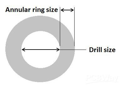
In a multilayer PCB, traces are routed from one layer to another layer with the help of vias. These vias are the holes drilled through copper pads on the surface of the PCB. The amount of copper left around the via on both top and bottom sides of the PCB is called the annular ring.

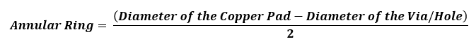
Mathematically, an annular ring is the difference between the diameter of the hole and diameter of the pad divided by 2. For instance, if the diameter of the pad is 24 mils and the diameter of the hole is 12 mils then the width of the annular ring is [(24-12)/2] = 6 mils
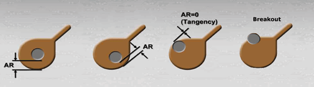
Calculation of the width of an annular ring plays an important role at the time of PCB manufacturing. If the width of the annular ring is not enough then the hole could touch the boundaries of the pad, this condition is called ‘Tangency’. In the extreme situation, the hole could be outside the boundary of the pad which is termed as ‘Breakout’. Both these situations should be avoided during the process of PCB fabrication.