Active Member
|
[China]

Address: Room 1520, Block 11, International E-Commerce Logistics Center, PingAn Road, PingHu Street, LongGang District, ShenZhen City, China 518111
Contact name:Steven YU

Witgain Technology Limited |
|
|
Ultra Thin 4 Layer Printed Circuit Board Immersion Gold Treatment
1 4 Layer Printed Circuit Board PCB .
2 Immersion Gold treatment, gold thickness 2u'.
3 FR4 substrate material, tg170 degree.
4 Min line space and width 3/3mil.
5 Copper thickness is H/H/H/H OZ
6 Green solder mask and white silkscreen.
7 ROHS, MSDS, SGS, UL, ISO9001&ISO14001 Certificated
1 FR4 substrate PCB : 2 Layer Printed Circuit Board, 4 Layer PCB, 6 Layer PCB, 8 Layer PCB, 10 Layer PCB, 12 Layer PCB, 14 Layer PCB, 16 Layer PCB, 18 Layer PCB, 20 Layer PCB, 22 Layer PCB, 24 Layer PCB, HDI PCB, High frequency PCB.
2 Aluminum Substrate pcb: 1 Layer Aluminum PCB, 2 Layer Aluminum PCB, 4 Layer Aluminum PCB.
3 Flexible PCB: 1 Layer FPC, 2 Layer FPC, 4 Layer FPC, 6 Layer FPC
4 Rigid-Flex PCB: 2 Layer Rigid-Flex PCB, 4 Layer Rigid-Flex PCB, 6 Layer Rigid-Flex pcb, 8 Layer Rigid-Flex PCB, 10 Layer Rigid-Flex pcb
5 Ceramic substrate pcb: single Layer Ceramic pcb, 2 layer ceramic pcb
| NO | Item | Capability |
| 1 | Layer Count | 1-24 Layers |
| 2 | Board Thickness | 0.1mm-6.0mm |
| 3 | Finished Board Max Size | 700mm*800mm |
| 4 | Finished Board Thickness Tolerance | +/-10% +/-0.1(<1.0mm) |
| 5 | Warp | <0.7% |
| 6 | Major CCL Brand | KB/NanYa/ITEQ/ShengYi/Rogers Etc |
| 7 | Material Type | FR4,CEM-1,CEM-3,Aluminum,Copper, Ceramic, PI, PET |
| 8 | Drill Hole Diameter | 0.1mm-6.5mm |
| 9 | Out Layer Copper Thickness | 1/2OZ-8OZ |
| 10 | Inner Layer Copper Thickness | 1/3OZ-6OZ |
| 11 | Aspect Ratio | 10:1 |
| 12 | PTH Hole Tolerance | +/-3mil |
| 13 | NPTH Hole Tolerance | +/-1mil |
| 14 | Copper Thickness of PTH Wall | >10mil(25um) |
| 15 | Line Width And Space | 2/2mil |
| 16 | Min Solder Mask Bridge | 2.5mil |
| 17 | Solder Mask Alignment Tolerance | +/-2mil |
| 18 | Dimension Tolerance | +/-4mil |
| 19 | Max Gold Thickness | 200u'(0.2mil) |
| 20 | Thermal Shock | 288℃, 10s, 3 times |
| 21 | Impedance Control | +/-10% |
| 22 | Test Capability | PAD Size min 0.1mm |
| 23 | Min BGA | 7mil |
| 24 | Surface Treatment | OSP, ENIG,HASL, Plating Gold, Carbon Oil,Peelable Mask etc |
Q1: What is a 4-Layer PCB Stackup?
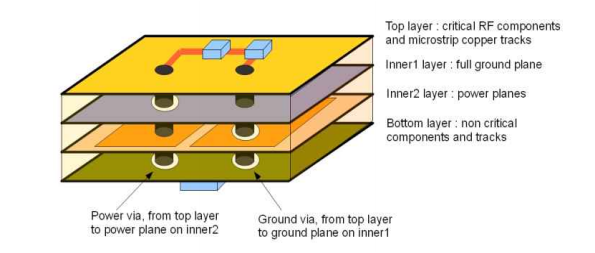
A1: A 4-layer PCB Stackup is a multilayer PCB that consists of multiple layers of copper and insulating materials stacked one above the other. For maximum efficiency and minimum losses and EMI, it is important to plan the right stack up of layers before starting the fabrication process. 4-layer PCB is the most common stack-up arrangement used in modern electronics.
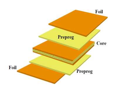
A 4-layer PCB stack up consists of top and bottom layers, a core (copper-clad layer), and an insulating layer also called prepreg made of a dielectric material like glass fiber/weave cloth. The top and bottom layers are made of copper foils, which are then laminated and etched to create slots for mounting the components. The core layer is made up of prepreg sandwiched between two copper foils. These top and bottom layers, core layer, and prepreg are bound together in such a way that no air is trapped between them.
As mentioned in the previous paragraph, the 4-layer PCB comprises the top and bottom layers, prepreg and a core layer. Now, the top and bottom layers, made of copper foils are used as signal planes. After lamination, the desired slots are etched for the placement of components and vias, which are electroplated holes connecting different planes in the PCB. The top side of the core is used as a ground plane, while the bottom side is used as a power plane. To reduce EMI and crosstalk, it is advisable to place the ground plane above the power plane. This will help in the reduction of overlapping and interference of the magnetic fields created by the signal and the current planes. The ground plane also helps in routing the return current and dissipation of heat.