

Active Member
|
[China]

Address: Room 1520, Block 11, International E-Commerce Logistics Center, PingAn Road, PingHu Street, LongGang District, ShenZhen City, China 518111
Contact name:Steven YU

Witgain Technology Limited |
|
|
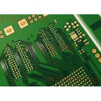
10 Layer Printed Circuit Boards Custom Printed Circuit Board
Main Features:
1 10 Layer PCB made from FR4 Material, high TG FR4, TG180, which has high stability.
2 The PCB is customized product. It was produced according to customoer's gerber design and requirement.
3 The solder mask is green solder mask and copper thickness is 1oz each layer.
4 The surface treatment is immersion gold and gold thickness is 2u'.
5 Need to use high TG prepreg during lamination, TG 180 Prepreg.
6 Used in industrial control area.
Our Production Capability:
| NO | Item | Capability |
| 1 | Layer Count | 1-24 Layers |
| 2 | Board Thickness | 0.1mm-6.0mm |
| 3 | Finished Board Max Size | 700mm*800mm |
| 4 | Finished Board Thickness Tolerance | +/-10% +/-0.1(<1.0mm) |
| 5 | Warp | <0.7% |
| 6 | Major CCL Brand | KB/NanYa/ITEQ/ShengYi/Rogers Etc |
| 7 | Material Type | FR4,CEM-1,CEM-3,Aluminum,Copper, Ceramic, PI, PET |
| 8 | Drill Hole Diameter | 0.1mm-6.5mm |
| 9 | Out Layer Copper Thickness | 1/2OZ-8OZ |
| 10 | Inner Layer Copper Thickness | 1/3OZ-6OZ |
| 11 | Aspect Ratio | 10:1 |
| 12 | PTH Hole Tolerance | +/-3mil |
| 13 | NPTH Hole Tolerance | +/-1mil |
| 14 | Copper Thickness of PTH Wall | >10mil(25um) |
| 15 | Line Width And Space | 2/2mil |
| 16 | Min Solder Mask Bridge | 2.5mil |
| 17 | Solder Mask Alignment Tolerance | +/-2mil |
| 18 | Dimension Tolerance | +/-4mil |
| 19 | Max Gold Thickness | 200u'(0.2mil) |
| 20 | Thermal Shock | 288℃, 10s, 3 times |
| 21 | Impedance Control | +/-10% |
| 22 | Test Capability | PAD Size min 0.1mm |
| 23 | Min BGA | 7mil |
| 24 | Surface Treatment | OSP, ENIG,HASL, Plating Gold, Carbon Oil,Peelable Mask etc |
FQA:
Q1: How to define a printed circuit board?
A1: A Printed Circuit Board or PCB is a board that is used to connect electrical components. The board is made out of Fiberglass, Epoxy and other laminated material with copper tracks in place of wires to make connections between components. Components like Microchips, Diodes, Resistors and Switches are soldered on to the board and the copper traces provide the electrical connections between them through conducting pathways.
Paul Eisler invented the printed circuit board (PCB) in 1936. Before the PCB was invented electronic components were connected with a number of wires and as a result took up a large amount of space. Printed Circuit Boards save considerable amounts of space as the boards are much more compact and are better organized. Thus, PCBs help make electronic and electrical systems smaller.
In addition to making circuits smaller, PCBs make it easier to repair circuits and identify any potential errors. They are low cost, highly reliable and immune to movement. Due to these advantages, they have become the de facto standard and are used in almost all electronic systems.


