.


Active Member
|
[China]

Address: Room 1520, Block 11, International E-Commerce Logistics Center, PingAn Road, PingHu Street, LongGang District, ShenZhen City, China 518111
Contact name:Steven YU

Witgain Technology Limited |
|
|
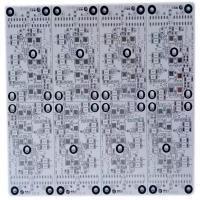
thermal conductive copper substrate 1 layer PCB
PCB Specifications:
Part NO: 04B2302176
Layers: 1Layer
Surface Finished: HASL
Material: copper sbstrate
Thickness: 1.6mm
PCB Size: 172.72 * 157.48 mm
Finished copper: 1OZ
Solder Mask colour: white
Silkscreen colour: black
Special Features: thermal conductive
Standard: IPC-A-600G Class II
Certificates: UL/94V-0/ISO
Our Product Categories:
| Our Product Categories | ||
| Material Kinds | Layer Counts | Treatments |
| FR4 | Single Layer | HASL Lead Free |
| CEM-1 | 2 Layer/Double Layer | OSP |
| CEM-3 | 4 Layer | Immersion Gold/ENIG |
| Aluminum Substrate | 6 Layer | Hard Gold Plating |
| Iron Substrate | 8 Layer | Immersion Silver |
| PTFE | 10 Layer | Immersion Tin |
| PI Polymide | 12 Layer | Gold fingers |
| AL2O3 Ceramic Substrate | 14 Layer | Heavy copper up to 8OZ |
| Rogers, Isola high frequency materials | 16 Layer | Half plating holes |
| Halogen free | 18 Layer | HDI Laser drilling |
| Copper based | 20 Layer | Selective immersion gold |
| 22 Layer | immersion gold +OSP | |
| 24 Layer | Resin filled in vias | |
FAQ:
Q:what is thermal conductivity?
A:
Your circuit board substrate and copper conductors are the primary factors that determine how heat will move around the board. Your components will generate heat during operation, illustrating the importance of estimating thermal conductivity of a PCB. The thermal properties of your circuit board substrate are one factor that determine temperature rise in your components (particularly junction temperature) and heat flux away from critical components.
In order to determine whether you should include active and passive thermal management measures in your printed circuit board, you can use some methods of estimating thermal conductivity of a PCB. This can help you estimate the temperature rise in your board using the power dissipation values for your components. Some simple layout and stackup choices in your circuit board can help change the temperature difference between various regions of your board, which helps ensure your printed circuit board operates at an acceptable temperature.
Thermal analysis is printed circuit board design is vital for ensuring desired performance and longevity of your next product. Your goal in circuit board design should be to design a system that provides the desired functionality over the longest possible lifetime. Understanding how to estimate thermal conductivity of a PCB and selecting the appropriate components that can operate under this condition will ensure your next printed circuit board remains reliable.
As components run in your circuit board and the junction temperature rises, the thermal resistance of your substrate will determine how heat transports to cooler areas of the board. If you know the thermal conductivity of your substrate and copper, you can estimate the effective thermal conductivity of your entire circuit board and calculate the approximate thermal resistance. In the event that your components generate too much heat and temperature rise is too great, you can determine whether to add a heat sink or some active cooling measures to your board in order to reduce the junction temperature in switching components.
As a fundamental property of any material, thermal conductivity defines the heat flux between hot and cold regions in your PCB. The thermal conductivity of your substrate material can be found in material datasheets. However, once you have an idea of your stackup and copper weight in your layout, you will want to calculate the effective thermal conductivity of your substrate. Formulas for calculating this directly vary depending on who you ask, although there are a number of lumped models in the literature. The simplest method is to use a weighted average based on the volume of copper and substrate material in your PCB:

Effective thermal conductivity estimate based on a volume weighted average of your PCB material parameters
The above equation shows a simple volume weighted average for calculating the effective thermal conductivity, where “s” indicates the substrate and “c” indicates copper. However, this is just a rough estimate, and you’ll get much more accurate results if you use a specialized 3D multiphysics simulator. Once you’ve determined the effective thermal conductivity of your PCB, you’re ready to calculate the thermal resistance in your board, which will give you some idea of how heat will transfer through your stackup.
Thermal resistance is influenced by the same structures that determine the effective thermal conductivity of your PCB. Traces, thermal pads, vias, plane layers, and your stackup materials will collectively determine the effective thermal conductivity. Once you’ve determined this, you can calculate the thermal resistance along the thickness direction with the following equation:

Thermal resistance equation
Similarly, you can calculate the thermal resistance of your board along the surface direction using the board’s cross sectional area. Finally, you can then calculate the heat flow rate in your board q, which is equal to the temperature gradient divided by the thermal resistance.
Reduce design time by eliminating your component creation process.
Using copper thermal reliefs and thermal pads on active components also helps remove heat into a copper plane or a heatsink, respectively. Once heat is transferred into a heatsink, it can be removed by taking advantage of airflow across the surface of the heatsink. When combined with proper stackup design and substrate material selection, you can reduce the number and/or size of active cooling measures you need to implement during PCB design.
Learn more about designing the perfect layer stack with Francesco Poderico.
Learn more about working with active cooling components in your PCB layout.

Stackup design for an HDI board
Thermal resistance is simply the thermodynamic analog of electrical resistance. The easiest way to reduce thermal resistance is to use a substrate with high thermal conductivity. Some common alternative substrate materials include ceramics, which have very high thermal conductivity compared to FR4. Another option is metal core PCBs, where the central core layer of the board is some metal with high conductivity.
Using thicker copper traces provides two benefits; first, thicker copper traces can carry more current for a given operating temperature. In other words, they will experience a lower temperature rise due to heat dissipation. Second, once copper traces do experience a temperature rise, heat diffuses away from conductors at a higher rate as copper has high thermal conductivity. Both aspects of copper conductors help reduce temperature rise in your board and make the temperature distribution more uniform.
Ceramic materials carry greater manufacturing costs due to the specialized processes they require, but they provide factors of 20 to 100 higher thermal conductivity compared to FR4. Metallic core substrates provide similarly high thermal conductivity. Any of these options are an excellent choice for moderately high frequency applications and will provide low thermal resistance. PTFE laminates with a metal core may be a better choice from the perspective of balancing dielectric losses and thermal management in microwave and mmWave applications.
Learn more about selecting the right substrate material for different applications.
Learn more about working with ceramic substrates for your next circuit board.
Learn more about working with aluminum substrates.

Polygon pour and thermal pad design in Altium Designer
Once you determine the effective thermal conductivity of your circuit board and calculate the thermal resistance, you’ll have an idea of the heat management methods you should use to ensure your board and components do not overheat. The layout and routing features in your PCB design software are the primary tools you’ll use to place components in the appropriate locations around the board.
If you plan to compensate for low effective thermal conductivity in a board on standard FR4, you’ll want to work with a design package that includes a long list of standard stackup materials and active cooling components. You’ll be able to select a substrate with sufficiently high thermal conductivity and start creating your layout. The best PCB design software will include these features and much more in a single program. This is exactly the environment that you’ll find in Altium Designer, the only fully integrated PCB design software platform.
Altium Designer includes an industry-standard layer stackup manager that allows you to customize the electrical and thermal properties of your substrate to match materials with high thermal conductivity. With the materials library in Altium Designer, you can easily select from a large number of common materials for use as your core, prepreg, and laminates. The layout and routing tools give you the power to design your board so that its thermal resistance is closer to your desired value. These tools and much more are accessible in a single platform, giving you a complete toolset for PCB design and analysis.
Altium Designer’s ultra-accurate layout and stackup tools are ideal for implementing the thermal management strategy your board needs. You can easily place components, add a thermal pad and heat sink to components, define copper pour regions, and many more tasks involved in thermal management design. With the PDNA extension, and you have a powerful analysis tool that aids thermal management. You can implement the right strategy to combat temperature rise in your PCB and transfer heat away from critical components in your PCB.
If you’ve never worked in an integrated design environment, rest assured that Altium will be there with the resources you need for success. You’ll have access to the AltiumLive forum, podcasts and webinars with industry experts, an extensive knowledge base full of design tips, and plenty of design tutorials. No other PCB design software company is this invested in your success.
Altium Designer has set a new standard in circuit board design and analysis. You can easily take control over all aspects of your next product and implement the right thermal management strategy with Altium Designer.
.


