Active Member
|
[China]

Address: Room 1520, Block 11, International E-Commerce Logistics Center, PingAn Road, PingHu Street, LongGang District, ShenZhen City, China 518111
Contact name:Steven YU

Witgain Technology Limited |
|
|
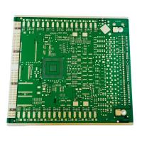
HDI circuit board FR4 TG170 substrate ENIG 2u' 10 Layer PCB
PCB Specifications:
Part NO: S10E5012A0
Layers: 10Layer
Surface Finished: Immersion gold 2u'
Material: FR4
Thickness: 1.8mm
PCB Size: 154mm*143mm
Finished copper: 1OZ
Solder Mask colour: Green
Silkscreen colour: White
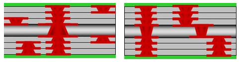
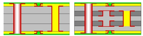
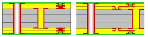
Blind hole size: 0.127mm (1-2/9-10)
Buried hole size:0.127mm (2-3/2-9/8-9)
Though hole size: 0.3mm (1-10)
No. of PP: 8pcs PP
Certificates: UL/94V-0/ISO
Our Product Categories:
| Our Product Categories | ||
| Material Kinds | Layer Counts | Treatments |
| FR4 | Single Layer | HASL Lead Free |
| CEM-1 | 2 Layer/Double Layer | OSP |
| CEM-3 | 4 Layer | Immersion Gold/ENIG |
| Aluminum Substrate | 6 Layer | Hard Gold Plating |
| Iron Substrate | 8 Layer | Immersion Silver |
| PTFE | 10 Layer | Immersion Tin |
| PI Polymide | 12 Layer | Gold fingers |
| AL2O3 Ceramic Substrate | 14 Layer | Heavy copper up to 8OZ |
| Rogers, Isola high frequency materials | 16 Layer | Half plating holes |
| Halogen free | 18 Layer | HDI Laser drilling |
| Copper based | 20 Layer | Selective immersion gold |
| 22 Layer | immersion gold +OSP | |
| 24 Layer | Resin filled in vias | |
FAQ:
Q:what is HDI PCB?
A:
High-density interconnect, or HDI, circuit boards are printed circuit boards with a higher wiring density per unit area than traditional printed circuit boards. In general, HDI PCBs are defined as PCBs with one or all of the following: microvias; blind and buried vias; built-up laminations and high signal performance considerations. Printed circuit board technology has been evolving with changing technology that calls for smaller and faster products. HDI boards are more compact and have smaller vias, pads, copper traces and spaces. As a result, HDIs have denser wiring resulting in lighter weight, more compact, lower layer count PCBs. Rather than using a few PCBs in a device, one HDI board can house the functionality of the previous boards used.
The primary benefit of HDI printed circuit boards is the capability to “do more with less”; with copper-etching technology continuously refined for better precision, it became possible to combine functionalities of multiple PCBs into one HDI PCB.
Shortening the distance between devices and trace spaces, HDI PCBs allow for deployment of a large number of transistors for better performance in electronics while lowering power consumption. Signal integrity is also improved due to the shorter distance connections and lower power requirements. Other performance improvements over conventional PCBs include stable voltage rail, minimal stubs, lower RFI/EMI, and closer ground planes and distributed capacitance.
Additionally, consider using a HDI printed circuit board for the following benefits:
Depending on the design requirements, HDI Printed Circuit Boards can utilize different layering methods to achieve the desired performance.
HDI PCB (1+N+1): Simplest HDI
HDI PCB (2+N+2): Moderate Complex HDI
ELIC (Every Layer Interconnection): Most Complex HDI