

Active Member
|
[China]

Contact name:Vicky Lee

Huaswin Electronics Co.,Limited |
|
|
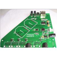
Consumer electronic Printed Circuit Board Assembly Through Hole PCB Assembly PCBA Service
Specifications
1. Our professional engineering team can put your project into production in a short time. Sample pictures and
BOM are needed to make customized products.Also we can supply for the copy of the PCB and PCBA ,so you
just sent me the enquiry is ok ,we can do what you need to do !
2. We can supply CAD and Pro-E designed precision moulds. Moulds can be designed and manufactured
according to customers' requests or samples. Plastic injection processing available.
3. Purchasing the electronic components for you to the production of the PCBA
4. We have advanced equipment for through-hole and SMT DIP COB cable Assembly
5. ROHS compliant and lead-free process.
6. In-circuit, functional tests& burn-in tests, full system test
7. High output to guarantee prompt delivery.
Welcome to Huaswin!
Huaswin Electronics is a professional PCB & PCB Assembly manufacturer, located in Shenzhen, China.
We supply one-stop facility services: PCB design, PCB fabrication, components procurement, SMT and DIP
assembly ,IC pre-programming / burning on-line, testing, anti-static packing.
PCB capability and services:
1. Single-sided, double-sided & multi-layer PCB (up to 30 layers)
2. Flexible PCB (up to 10 layers)
3. Rigid-flex PCB (up to 8 layers)
4. CEM-1, CEM-3 FR-4, FR-4 High TG, Polyimide, Aluminum-based material.
5. HAL, HAL lead free, Immersion Gold/ Silver/Tin, Hard Gold, OSP surface treatment.
6. Printed Circuit Boards are 94V0 compliant, and adhere to IPC610 Class 2 international PCB standard.
7. Quantities range from prototype to volume production.
8. 100% E-Test
Detailed Specification of PCB Manufacturing
1 | layer | 1-30 layer |
2 | Material | CEM-1, CEM-3 FR-4, FR-4 High TG, Polyimide, Aluminum-based material. |
3 | Board thickness | 0.2mm-6mm |
4 | Max.finished board size | 800*508mm |
5 | Min.drilled hole size | 0.25mm |
6 | min.line width | 0.075mm(3mil) |
7 | min.line spacing | 0.075mm(3mil) |
8 | Surface finish | HAL, HAL Lead free,Immersion Gold/ Silver/Tin, Hard Gold, OSP |
9 | Copper thickness | 0.5-4.0oz |
10 | Solder mask color | green/black/white/red/blue/yellow |
11 | Inner packing | Vacuum packing,Plastic bag |
12 | Outer packing | standard carton packing |
13 | Hole tolerance | PTH:±0.076,NTPH:±0.05 |
14 | Certificate | UL,ISO9001,ISO14001,ROHS,TS16949 |
15 | Profiling punching | Routing,V-CUT,Beveling |
PCB Assembly services:
SMT Assembly
Automatic Pick & Place
Component Placement as Small as 0201
Fine Pitch QEP - BGA
Automatic Optical Inspection
Through-hole Assembly
Wave Soldering
Hand Assembly and Soldering
Material Sourcing
IC pre-programming / Burning on-line
Function testing as requested
Aging test for LED and Power boards
Complete unit assembly (which including plastics, metal box, Coil, cable assembly etc)
Packing design
Conformal coating
Both dip-coating and vertical spray coating is available. Protecting non-conductive dielectric layer that is
applied onto the printed circuit board assembly to protect the electronic assembly from damage due to
contamination, salt spray, moisture, fungus, dust and corrosion caused by harsh or extreme environments.
When coated, it is clearly visible as a clear and shiny material.
Complete box build
Complete 'Box Build' solutions including materials management of all components, electromechanical parts,
plastics, casings and print & packaging material
Testing Methods
AOI Testing
· Checks for solder paste
·
Checks for components down to 0201"
·
Checks for missing components, offset, incorrect parts, polarity
X-Ray Inspection
X-Ray provides high-resolution inspection of:
· BGAs
· Bare boards
In-Circuit Testing
In-Circuit Testing is commonly used in conjunction with AOI minimizing functional defects caused by
component problems.
· Power-up Test
· Advanced Function Test
· Flash Device Programming
· Functional testing
Detailed Specification of Pcb Assembly
1 | Type of Assembly | SMT and Thru-hole |
2 | Solder Type | Water Soluble Solder Paste,Leaded and Lead-Free |
3 | Components | Passives Down to 0201 Size |
BGA and VFBGA | ||
Leadless Chip Carries/CSP | ||
Double-Sided SMT Assembly | ||
Fine Pitch to 08 Mils | ||
BGA Repair and Reball | ||
Part Removal and Replacement-Same Day Service | ||
3 | Bare Board Size | Smallest:0.25x0.25 Inches |
Largest:20x20 Inches | ||
4 | File Formats | Bill of Materials |
Gerber Files | ||
Pick-N-Place File(XYRS) | ||
5 | Type of Service | Turn-Key,Partial Turn-Key or Consignment |
6 | Component Packaging | Cut Tape |
Tube | ||
Reels | ||
Loose Parts | ||
7 | Turn Time | 15 to 20 days |
8 | Testing | AOI inspection |
X-Ray inspection | ||
In-Circuit testing | ||
Functional test |


