
|
|
[China]

Trade Verify
Address: Room 1106, CIBC, No.198 Wuxing Rd, Hangzhou, P.R.China
Contact name:Xu

Hangzhou Freqcontrol Electronic Technology Ltd. |
|
Verified Suppliers
|
|
|
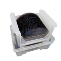
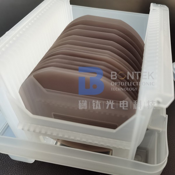
Fe Doped Yellow Black LiTaO3 Wafer for High-Density Holographic Information Storage
Lithium Tantalate (LiTa03) is widely used in the optical fields for optical modulation, optical recording, and frequency conversion because of its electro-optic,acousto-optic,piezoelectric,thermal-optic and photorefractive effects. With the rapidly growing demand for higher information storage capacity, Fe doped Lithium Tantalate (Fe:LiTaO3) is introduced as a solution to high-density and high-capacity holographic information storage.


Diameter | 76.2±0.2mm | 100±0.2mm | 150±0.2mm | ||||
Primary Flat | 22±1mm | 32±1mm | 47.5mm, 57.5mm, Notch | ||||
Orientation | 36°Y, 42°Y, X-112°Y, Y, Z | ||||||
Thickness | 0.07mm~1.0mm | 0.1mm~1.0mm | 0.35mm~1.0mm | ||||
Surface finish | Single / Double side polish / Double side lapped | ||||||
TTV | < 1~5µm | ||||||
BOW | ± (20µm ~40um ) | ||||||
Warp | <= 20µm ~ 50µm | ||||||
LTV (5mmx5mm) | <1.5 um | ||||||
PLTV(<0.5um) | ≥98% (5mm*5mm) with 2mm edge excluded | ||||||
Polished side Ra | Roughness Ra<=5A | ||||||
Back Side Criteria | Roughness Ra:0.5-1.0µm, GC#1000 | ||||||
Scratch & Dig (S/D) | 20/10, 40/20, 60/40 | ||||||
Edge Profile | Compl't with SEMI M1.2@with GC800# .regular at C typed | ||||||
Cracks, saw marks, stains | None | ||||||
Properties | LiTaO3 (LT) |
Type of Material | Single Crystal |
Crystal Structure | Trigonal,a = 5.154, c = 13.784Å |
Melting Point | 1650℃ |
Curie Temperature | 607℃ |
Transmission Range | 400 – 5000 nm |
Absorption edge | 270nm |
Absorption loss | < 0.15 %/cm @ 1064 nm |
Refractive Index | no=2.176,ne=2.180(at 0.633 µm) |
no=2.131,ne=2.134(at 1.2 µm) | |
Density | 7.45g/cm3 |
Thermal Conductivity | 8.78x 10⁻⁷ m2/sec |
Optical homogeneity | ~10-5 |
Hardness (Mohs) | 5 |
Elastic Coefficient | CE11 2.33(X 1011 N/m2) |
CE33 2.77(X 1011 N/m2) | |
Dielectric Constant | ε11/ε0 52.7 |
ε33/ε0 44.5 | |
Solubility in Water | insoluble in water |
NLO Coefficients | d33 = 13.8 pm/V |
d22= 2.4 pm/V | |
d11= 0.85 pm/V | |
Electro-Optic Coefficients | r31 =8.4 pm/V, @633nm |
r22 =20 pm/V, @633nm | |
r33 =30.5 pm/V, @633nm | |
Damage Threshold | 2 MW/cm2@532nm |


FAQs:
A: We look at ourselves as the piezo wafer specialist. We are the very first to work with Single Crystal Quartz in China about 30 years ago. Then gradually we step in the field of LiNbO3, LiTaO3, Quartz glass, LGS, CTGS etc. Especially, if you are looking for a piezo quartz supplier, we are the ultimate choice! We export millions of quartz blanks each year because we master the AT, SC and IT cuts with superior angle precision.
A: Yes, of course. We can fabricate as per your request. In addition, we are so experienced with piezo wafers that we can provide you relevant suggestions if you are not 100% sure about your choice. Besides, we do have some standard wafers in stock, please check with us.
A: Yes, we would suggest you go with the courier agent you are most familiar with (DHL, FedEX, UPS etc.). We can ship via your account. And, of course, we will pack the products safely in acceptable size to help you save the shipping cost. If you need us to take care of the freight, it’s also not a problem. We also have good discount with the international courier companies.
A: The wafer products are fragile and sometimes expensive. The last thing, as the manufacturer, we want to see is the products we make were damaged during courier. As a result, we will pack the wafers adequately and put them in a proper carton filled with buffer sponge. However, accidents are inevitable sometimes. So, please follow the “Acceptance check” steps shown in the drawings below. If the unwanted happened, we will either give the replenishment or refund if you follow the checking steps.
A: Sure. Factory inspection is important for large quantity purchase and long-term cooperation. Face to face discussion is what we mostly confident with. During the past years, big names around the world have witnessed our progress in factory build-up. These days, due to the Covid-19 pandemic, we also had the experience of videoconferencing with global buyers.
Acceptance Check


