
|
|
[China]

Trade Verify
Address: Room 1106, CIBC, No.198 Wuxing Rd, Hangzhou, P.R.China
Contact name:Xu

Hangzhou Freqcontrol Electronic Technology Ltd. |
|
Verified Suppliers
|
|
|
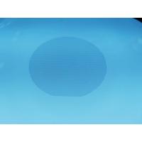
High Resistance Single Side Polished LED Sapphire Wafer with BOW 10um
Sapphire Wafer is a kind of sapphire slice that has been precision cut from a sapphire boule to the required dimensions. It is widely used for various applications in the optoelectronics, electronics, and semiconductor industries. Sapphire Wafer has excellent thermal conductivity, high thermal shock resistance, high dielectric strength, and excellent optical properties, making it ideal for high reliability applications. Its mechanical properties are superior to those of quartz and optical glass. The features of Sapphire Wafer include bow & warp of ≤20μm, diameter of 2inch-8inch, perpendicularity of ≤3 Arc Min, TTV of ≤3μm and single side polished surface quality.
| Sapphire Wafer | |||
| Item | 2 Inch | 4 Inch | 6 Inch |
| Crystal | LED Grade Sapphire | LED Grade Sapphire | LED Grade Sapphire |
| Purity | >99.998% | >99.998% | >99.998% |
| Color | Transparent | Transparent | Transparent |
| Orientation | C plane tiled M axis 0.20°±0.1° | C plane tiled M axis 0.20°±0.1° | C plane tiled M axis 0.20°±0.1° |
| Diameter | 50.8±0.1mm | 100±0.2mm | 150±0.2mm |
| Thickness | 430±15um | 650±25um | 1300±25um |
| PF Location | A-axist±0.2° | A-axist±0.2° | A-axist±0.2° |
| Flat Length | 16.0±1.0mm | 30.0±1.0mm | 49.0±1.0mm |
| Front Side Surface | Mirror polished EPI-Ready | Mirror polished EPI-Ready | Mirror polished EPI-Ready |
| Surface Roughness | Ra<3A | Ra<3A | Ra<3A |
| Back Side Roughness | Fine ground, Ra=1.0±0.2um | Fine ground, Ra=1.0±0.2um | Fine ground, Ra=1.0±0.2um |
| TTV | <5.0um | <10um | <15um |
| BOW | 0~-5um | 0~-10um | 0~-30um |
| Warp | <10um | <15um | <40um |
| Bubble& Color | None by visual inspection in fluorescent light | ||
| Cleanliness | Free visible contamination | ||
| Packaging | Vacuum packed in one-piece box or Entegris cassettes of 25 | ||

BonTek's Sapphire Plate and Sapphire Wafer are widely used in various fields, such as optical communications, medical treatments, optoelectronics, aerospace, military, and more. With ISO:9001 certification, our products guarantee superior quality. We offer Minimum Order Quantity of 10 pcs, with a Price of $60.00/ea. Our product is provided in a Cassette, vacuum sealed package, with Delivery Time of 2~4 weeks. We accept TT/in Advance payment terms, and have a Supply Ability of 10000 pcs. Our Sapphire Plate and Sapphire Wafer have a Surface Roughness of Ra<0.2nm, Clear Aperture of more than 90%, and Diameter of 2inch-8inch. Our product also provides excellent Perpendicularity of ≤3 Arc Min and Flatness of λ/10.
Sapphire wafers are shipped in sealed containers to ensure the product is not damaged during shipment. Packaging materials used to ensure that the wafers remain intact include bubble wrap, anti-static bags, and foam protectors. For international shipping, we also use custom designed containers to reduce the chance of damage due to shock or vibration.
For customers who require special handling, we use special packaging materials and techniques to ensure the product is not damaged in transit. We also offer overnight shipping and other special services to meet customer needs.
When shipping sapphire wafers, we take extra precautions to ensure that the product arrives safely and in a timely manner. We use only the best shipping methods and ensure that all customs paperwork is completed accurately and on time.


