
|
|
[China]

Trade Verify
Address: Room 1106, CIBC, No.198 Wuxing Rd, Hangzhou, P.R.China
Contact name:Xu

Hangzhou Freqcontrol Electronic Technology Ltd. |
|
Verified Suppliers
|
|
|
8 Inch Borofloat 33 Glass Wafer For Electronics, Optics, And Semiconductors
Borofloat 33 Glass Wafer Description
Borofloat 33 is a type of borosilicate glass that is widely used in various industries, including electronics, optics, and semiconductors. It is known for its excellent thermal and chemical properties, making it suitable for applications that require high temperature resistance and chemical durability.
Glass wafers made from Borofloat 33 are commonly used as substrates in the fabrication of electronic devices, such as MEMS (Microelectromechanical Systems) devices, sensors, and displays. They provide a flat and uniform surface for the deposition of thin films and other semiconductor processes.
These glass wafers are available in various sizes and thicknesses to accommodate different manufacturing requirements. The typical wafer sizes range from a few millimeters to several inches in diameter. The thickness can vary from a few micrometers to several millimeters.
Borofloat 33 Glass Wafer Parameters
| Material | BOROFLOAT 33 |
| Density (@ 25°C/77°F) | 2.23 g/cm3 |
| Modulus of Elasticity | 63 kN/mm2 |
| Knoop Hardness HK 0.1/20 | 480 |
| Poisson’s Ratio | 0.2 |
| Dielectric Constant (@ 1 MHz & 25°C) | 4.6 |
| Loss Tangent (@ 1 MHz & 25°C) | 37 x 10-4 |
| Dielectric Strength(@ 50 Hz & 25°C) | 16 kV/mm |
| Refractive Index (nd) | 1.472 |
| Dispersion (nF - nC) | 71.9 x 10⁻⁴ |
Borofloat 33 Glass Wafer Specifications
| Specification | 3” | 4” | 5" | 6" | 8" |
| Diameter | 76.2mm | 100mm | 125mm | 150mm | 200mm |
| Tol(±) | <0.1~0.25 mm | ||||
| Thickness | >0.10mm | >0.10mm | >0.30mm | >0.30mm | >0.30mm |
| Primary Flat | 22mm | 32.5mm | 42.5mm | 57.5mm | Notch |
| Notch | |||||
| TTV | <8um | <10um | <15um | <20um | <30um |
| Bow | ±20um | ±25um | ±40um | ±40um | ±60um |
| Warp | <30um | <40um | <50um | <50um | <60um |
| PLTV(<0.5um) | ≥95%(5mm*5mm) | ||||
| Transmittance | UV, Optical, IR or Custom option | ||||
| Edge Rounding | Compliant with SEMI M1.2 Standard/refer to IEC62276 | ||||
| Surface Type | Single Side Polished /Double Sides Polished | ||||
| Polished side Ra | <1.0nm or specific per requested | ||||
| Back Side Criteria | General is 0.2-0.5µm or as customized | ||||
| Appearance | Contamination | None | |||
| Particles>0.3µm | <=30 | ||||
| Saw Marks, striations | None | ||||
| Scratch | None | ||||
| Cracks, saw marks, stains | None | ||||
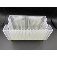
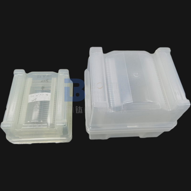
Glass Wafer Photos


FAQs:
A: We look at ourselves as the piezo wafer specialist. We are the very first to work with Single Crystal Quartz in China about 30 years ago. Then gradually we step in the field of LiNbO3, LiTaO3, Quartz glass, LGS, CTGS etc. Especially, if you are looking for a piezo quartz supplier, we are the ultimate choice! We export millions of quartz blanks each year because we master the AT, SC and IT cuts with superior angle precision.
A: Yes, of course. We can fabricate as per your request. In addition, we are so experienced with piezo wafers that we can provide you relevant suggestions if you are not 100% sure about your choice. Besides, we do have some standard wafers in stock, please check with us.
A: Yes, we would suggest you go with the courier agent you are most familiar with (DHL, FedEX, UPS etc.). We can ship via your account. And, of course, we will pack the products safely in acceptable size to help you save the shipping cost. If you need us to take care of the freight, it’s also not a problem. We also have good discount with the international courier companies.
A: The wafer products are fragile and sometimes expensive. The last thing, as the manufacturer, we want to see is the products we make were damaged during courier. As a result, we will pack the wafers adequately and put them in a proper carton filled with buffer sponge. However, accidents are inevitable sometimes. So, please follow the “Acceptance check” steps shown in the drawings below. If the unwanted happened, we will either give the replenishment or refund if you follow the checking steps.
A: Sure. Factory inspection is important for large quantity purchase and long-term cooperation. Face to face discussion is what we mostly confident with. During the past years, big names around the world have witnessed our progress in factory build-up. These days, due to the Covid-19 pandemic, we also had the experience of videoconferencing with global buyers.
Acceptance Check


