
|
|
[China]

Trade Verify
Address: Room 1106, CIBC, No.198 Wuxing Rd, Hangzhou, P.R.China
Contact name:Xu

Hangzhou Freqcontrol Electronic Technology Ltd. |
|
Verified Suppliers
|
|
|
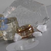
Quartz Crystal Piezoelectric Wafer Precision Substrates for Electrical Optical and Timing Applications
Quartz crystal wafers, also known as quartz substrates or quartz plates, are widely used in various electronic and optical applications. These synthetic quartz exhibits exceptional properties such as high purity, excellent electrical characteristics, and remarkable mechanical stability.
Quartz Crystal Properties
Quartz crystal wafers is with outstanding piezoelectric properties. Quartz can generate an electric charge when subjected to mechanical stress or vibrations, and vice versa. This property makes quartz crystal wafers highly desirable for applications involving precise timing, frequency control, and sensing. They serve as the foundation for quartz crystal oscillators and resonators used in electronic devices, such as watches, smartphones, computers, and communication systems.
Quartz crystal wafers have exceptional dimensional stability. The low coefficient of thermal expansion, meaning their dimensions remain relatively constant across a wide temperature range. This property makes them highly suitable for applications requiring stability and accuracy
Quartz crystal wafers have excellent optical transparency. They exhibit high transmission of light across a broad range of wavelengths, from ultraviolet (UV) to infrared (IR). This optical clarity makes them suitable for use in optical windows, lenses, prisms, and other components used in lasers, spectroscopy, microscopy, and other optical systems.


Quartz Crystal Details
| Property | Description |
|---|---|
| Chemical Formula | SiO2 |
| Crystal System | Hexagonal |
| Density | Typically 2.65 g/cm3 |
| Hardness | 7 on the Mohs scale |
| Transparency | Excellent transparency from ultraviolet (UV) to infrared (IR) |
| Refractive Index | Typically around 1.544 (at 589 nm) |
| Thermal Conductivity | 1.4 W/(m·K) |
| Coefficient of Expansion | 5.5 x 10^-7 /°C (parallel to C-axis) |
| Melting Point | Approximately 1,710°C |
| Electrical Properties | Piezoelectricity, low electrical conductivity, high dielectric constant |
| Applications | Quartz crystal oscillators, resonators, sensors, optics, timing devices, scientific instruments, telecommunications |
Crystal | Lithium Niobate | Lithium Tantalate | Quartz Crystal |
Diameter | 3’’, 4’’, 6’’, 8’’ | 3’’, 4’’, 6’’ | 3’’, 4’’, 5’’, 6’’, 8’’ |
Orientation | X / Y / Y41 / Y64/Y128 | X / X112 / YZ Y28 / Y36 / Y42 | X / Y / Z AT / ST |
Surface Finish | Single / Double sides polish (SSP/DSP) | ||
Thickness | 0.08mm / 0.25mm / 0.35mm / 0.50mm / 1.00mm / 2.00mm | ||
LTV | < 1.5um | ||
PLTV | >98% (5mm*5mm) | ||
TTV | < 5um | ||
Bow | -25um < bow < +25um | ||
Warp | < 35um | ||
Curie Temperature | 1142℃ ± 2℃ | 605℃ ± 2℃ | 573℃ |
Edge | CompI’t with SEMI M1.2 @ with GC#1000 | ||
Flat | 22±2mm, 32.5±2mm, 47.5±2mm, 57.5±2mm, Notch As per request | ||
Doping | Er, MgO | Fe | with or without seed |
Front Side | Roughness Ra< 1nm | ||
Back Criteria | Roughness Ra: 0.5--1.0um GC#1000 | ||
Contamination | Particles @ >0.3 micron | ||
Appearance | No Cracks, saw marks, stains | ||
Single Domian | Completed Polarization / Reduced | No Stress | |


FAQs:
A: We look at ourselves as the piezo wafer specialist. We are the very first to work with Single Crystal Quartz in China about 30 years ago. Then gradually we step in the field of LiNbO3, LiTaO3, Quartz glass, LGS, CTGS etc. Especially, if you are looking for a piezo quartz supplier, we are the ultimate choice! We export millions of quartz blanks each year because we master the AT, SC and IT cuts with superior angle precision.
A: Yes, of course. We can fabricate as per your request. In addition, we are so experienced with piezo wafers that we can provide you relevant suggestions if you are not 100% sure about your choice. Besides, we do have some standard wafers in stock, please check with us.
A: Yes, we would suggest you go with the courier agent you are most familiar with (DHL, FedEX, UPS etc.). We can ship via your account. And, of course, we will pack the products safely in acceptable size to help you save the shipping cost. If you need us to take care of the freight, it’s also not a problem. We also have good discount with the international courier companies.
A: The wafer products are fragile and sometimes expensive. The last thing, as the manufacturer, we want to see is the products we make were damaged during courier. As a result, we will pack the wafers adequately and put them in a proper carton filled with buffer sponge. However, accidents are inevitable sometimes. So, please follow the “Acceptance check” steps shown in the drawings below. If the unwanted happened, we will either give the replenishment or refund if you follow the checking steps.
A: Sure. Factory inspection is important for large quantity purchase and long-term cooperation. Face to face discussion is what we mostly confident with. During the past years, big names around the world have witnessed our progress in factory build-up. These days, due to the Covid-19 pandemic, we also had the experience of videoconferencing with global buyers.
Acceptance Check


