|
|
[China]

Trade Verify
Address: Room 1106, CIBC, No.198 Wuxing Rd, Hangzhou, P.R.China
Contact name:Xu

Hangzhou Freqcontrol Electronic Technology Ltd. |
|
Verified Suppliers
|
|
|
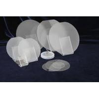
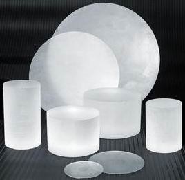
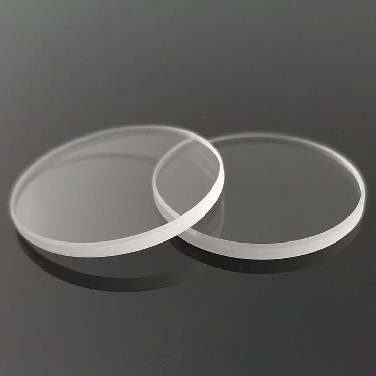
2Inch-6 Inch LED Grade Sapphire Crystal Substrate
Sapphire (molecular formula Al2O3) single crystal is an excellent multifunctional material. It has high temperature resistance, good heat conduction, high hardness, infrared penetration and good chemical stability. Widely used in industry, national defense and scientific research in many fields (such as high temperature resistant infrared window, etc.). At the same time, it is also a kind of single crystal substrate material with a wide range of uses. It is the preferred substrate in the blue, purple, white light emitting diode (LED) and blue laser (LD) industry at present (gallium nitride film needs to be epitaxed on the sapphire substrate first), as well as an important superconducting thin film substrate.
Orientation Cut | R-plane, C-plane, A-plane, M-plane or a specified orientation |
Orientation Tolerance | ± 0.3° |
Diameter / Size | 2 inches, 3 inches, 4 inches, 6 inches, 8 inches or others |
Diameter Tolerance | ± 0.2mm |
Thickness | 0.25mm, 0.33mm, 0.43mm, 0.65mm, 1mm or others; |
Thickness Tolerance | ± 25μm |
Primary Flat Length | 16.0±1.0mm for 2 inches, 22.0±1.0mm for 3 inches, 30.0±1.5mm for 4 inches, 47.5/50.0±2.0mm for 6 inches |
Primary Flat Orientation | A-plane (1 1-2 0 ) ± 0.2°; C-plane (0 0-0 1 ) ± 0.2°, Projected C-Axis 45 +/- 2° |
TTV | ≤10µm for 2 inches, ≤15µm for 3 inches, ≤20µm for 4 inches, ≤25µm for 6 inches |
BOW | ≤10µm for 2 inches, ≤15µm for 3 inches, ≤20µm for 4 inches, ≤25µm for 6 inches |
Front Surface | Epi-Polished (Ra< 0.3nm for C-plane, 0.5nm for other orientations) |
Back Surface | Fine ground (Ra=0.6μm~1.4μm) or Epi-polished |
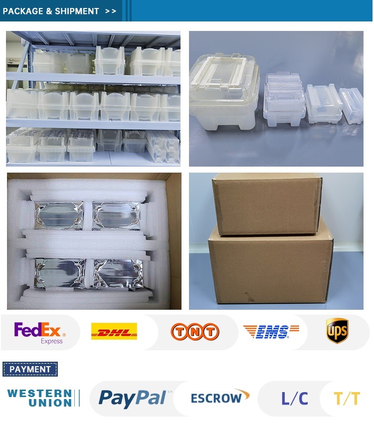
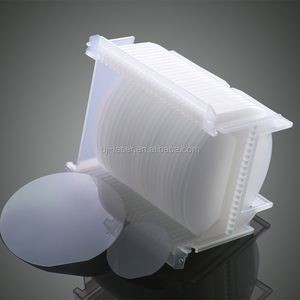
Packaging | Packaged in a class 100 clean room environment |