
|
|
[China]

Trade Verify
Address: Room 1106, CIBC, No.198 Wuxing Rd, Hangzhou, P.R.China
Contact name:Xu

Hangzhou Freqcontrol Electronic Technology Ltd. |
|
Verified Suppliers
|
|
|
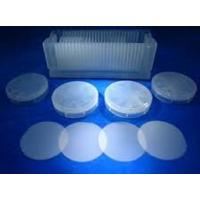
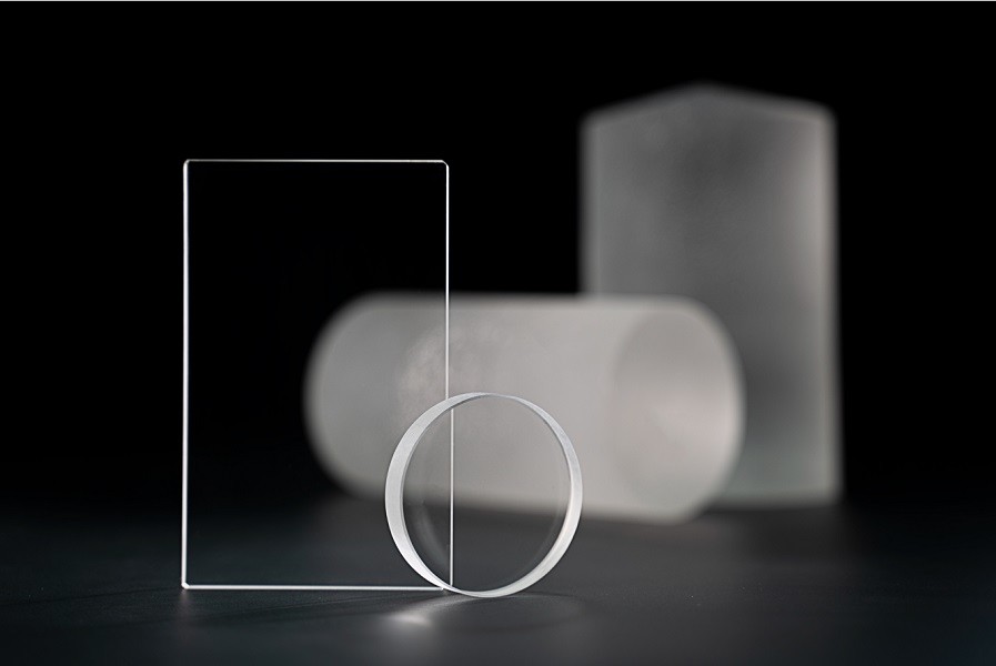
C Plane High Smoothness And High Cleanliness Sapphire Substrate For Semiconductor
Sapphire wafers are mainly suitable for the research and development of new semiconductor devices, offering high specifications such as high smoothness and high cleanliness in addition to the traditional sapphire substrate standard grades.
Main Features
• High strength, high hardness, high wear resistance (hardness second only to diamond)
• High transmittance (light transmittance in the ultraviolet to infrared range)
• High corrosion resistance (high tolerance to acid, alkali, plasma)
• High insulation (insulator, not easy to conduct electricity)
• High heat resistance (melting point 2050℃) Heat conductivity (40 times of glass)
Specification
• Standard size (φ2 ",3 ",4 ",6 ",8 ",12 "), other special size, corner shape and other shapes can be corresponding.
• Can correspond to a variety of plane orientation: c-plane, r-plane, m-plane, a-plane
• Double-sided grinding, single-sided grinding
• Customizable punching


| Crystal Materials | 99,996% of Al2O3,High Purity, Monocrystalline, Al2O3 | ||||
| Crystal quality | Inclusions, block marks, twins, Color, micro-bubbles and dispersal centers are non-existent | ||||
| Diameter | 2inch | 3inch | 4inch | 5inch ~ 7inch | |
| 50.8± 0.1mm | 76.2±0.2mm | 100±0.3mm | In accordance with the provisions of standard production | ||
| Thickness | 430±15µm | 550±15µm | 650±20µm | Can be customized by customer | |
| Orientation | C- plane (0001) to M-plane (1-100) or A-plane(1 1-2 0) 0.2±0.1° /0.3±0.1°, R-plane (1-1 0 2), A-plane (1 1-2 0 ), M-plane(1-1 0 0), Any Orientation , Any angle | ||||
| Primary flat length | 16.0±1mm | 22.0±1.0mm | 32.5±1.5 mm | In accordance with the provisions of standard production | |
| Primary flat Orientation | A-plane (1 1-2 0 ) ± 0.2° | ||||
| TTV | ≤10µm | ≤15µm | ≤20µm | ≤30µm | |
| LTV | ≤10µm | ≤15µm | ≤20µm | ≤30µm | |
| TIR | ≤10µm | ≤15µm | ≤20µm | ≤30µm | |
| BOW | ≤10µm | ≤15µm | ≤20µm | ≤30µm | |
| Warp | ≤10µm | ≤15µm | ≤20µm | ≤30µm | |
| Front Surface | Epi-Polished (Ra< 0.2nm) | ||||
| Back Surface | Fine ground (Ra=0.5 to 1.2 µm), Epi-Polished (Ra< 0.2nm) | ||||
| Note | Can provide high-quality sapphire substrate wafer according to customers' specific requirement | ||||
PHYSICAL PROPERTIES
| Density | 3.97 g/cm3 |
| Melting Point | 2040 degrees C |
| Thermal Conductivity | 27.21 W/(m x K) at 300 K |
| Thermal Expansion | 5.6 x 10 -6 /K (parallel C-axis) & 5.0 (perpendicular C-axis) x 10 -6 /K |
| Hardness | Knoop 2000 kg/mm 2 with 2000g indenter |
| Specific Heat Capacity | 419 J/(kg x K) |
| Dielectric Constant | 11.5 (parallel C-axis) 9.4 (perpendicular C-axis) at 1MHz |
| Young's Modulus (E) | 335 GPa |
| Shear Modulus (G) | 148.1 GPa |
| Bulk Modulus (K) | 240 GPa |
| Elastic Coefficients | C11=496 C12=164 C13=115 C33=498 C44=148 |
| Apparent Elastic Limit | 275 MPa (40,000 psi) |
| Poisson Ratio | 0.25 |
Acceptance Check


