
|
|
[China]

Trade Verify
Address: RM1510, YUNHUA TIMES, Shajing Street, Baoan District, Shenzhen,Guangdong, China
Contact name:Yang

Huashengxin Circuit Limited |
|
Verified Suppliers
|
|
|
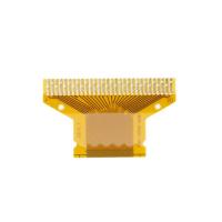
2 Sided Flexible Circuit Board Fast Turn Pcb HASL 4mil 0.1mm
Flex PCB Board 2 Sided Flexible Circuits PCB PCBA PCBA Board PCB Supplier Fast Turn Flexible PCB
Double Layer Flexible Circuits
Flexible circuits (also called as flex circuits, flexible printed circuit boards, flex PCB, etc) are consisted of a thin insulating polymer film having conductive circuit patterns affixed thereto and typically supplied with a thin polymer coating to protect the conductor circuits. The technology has been used for interconnecting electronic devices since long long time ago. It is now one of the most important interconnection technologies in use for the manufacture of many advanced electronic products.
In practice there are many different kinds of flexible circuits, including one metal layer, double sided, multilayer and rigid flex circuits. The circuits can be formed by etching metal foil cladding (normally of copper) from polymer bases, plating metal or printing of conductive inks among other processes.
Advantage:
1)Accuracy of designs. Most of the advanced electronic devices in
use today use flexible circuit boards because of the high level of
precision expected of them.
2)They are lightweight. The circuit boards can be folded easily,
thus they can be positioned in compartments.
3)Long-term performance. The superior qualities of flexible circuit
boards allow them to have durability and long-term performance. The
characteristics of low ductility and mass contained in these boards
allow them to overcome the influence of vibrations, therefore
giving them the capacity to have improved performance.
4)Heat dissipation. Because of the compact designs of the circuit
board, there are shorter thermal paths generated and the
dissipation of heat is faster compared to other kind of PCBs.
5)Flexibility. Due to their ability to be flexible, it is easily to
bend flexible circuit boards to various levels when installing
them, thus make it possible to enhance the functionality levels of
various electronics.
| FPC Technology Capability | |||
| Attribute (All dimensions are mils unless otherwise specified) | Mass Production (Yield≥ 80%,Cpk≥1.33) | Small Amount(Yield≥60%, Key Specification Yield≥80% | Sample |
| FPC(yes/no) | yes | yes | yes |
| Layer count/Structure, Max. | 2 | 4 | 6 |
| Size(L×W), Max. | 550mm*250mm | 550mm*250mm | 700mm*250mm |
| Nominal thickness (mm) | 0.1~0.5 | 0.1~0.5 | 0.1~0.8 |
| Thickness tolerance | ±10%(>0.3mm)/±0.03mm(≤0.3mm) | ±10%(>0.3mm)/±0.03mm(≤0.3mm) | ±10%(>0.3mm)/±0.03mm(≤0.3mm) |
| Surface finish type | ENIGENEPIGOPSI-SilverI-Tin HASLHard Gold | ENIGENEPIGOPSI-SilverI-Tin HASLHard Gold | ENIGENEPIGOPSI-SilverI-Tin HASLHard Gold |
| Soft ENIG(yes/no) | no | no | no |
| Base material type | PI | PI | PILCPTK |
| Coverlay thickness (um) | 28/50/60/80 | 28/50/60/80 | 28/50/60/80 |
| Adhesive thickness (um) | 25/40/50/65 | 25/40/50/65 | 25/40/50/65 |
| Copper thickness, Min./Max. (um) | 12-70 | 12-70 | 12-70 |
| Base material thickness, Min./Max. (um) | 25-75 | 25-75 | 25-100 |
| Mechanical drilled thru-hole size (DHS), Min. | 0.15 | 0.15 | 0.15 |
| Plating aspect ratio, Max. | 3:1 | 3:1 | 5:1 |
| Pad size, Min. | With through hole:0.4mm Without through hole:0.2mm | With through hole:0.4mm Without through hole:0.2mm | With through hole:0.3mm Without through hole:0.2mm |
| Pad size tolerance | 20% | 20% | 10% |
| Pad to pad space, Min. | 4mil | 4mil | 4mil |
| Pad to outline tolerance | ±3mil | ±3mil | ±2mil |
| Pattern location accurancy | ±3mil | ±3mil | ±2mil |
| Pattern location accurancy from top side to bottom | ±3mil | ±3mil | ±2mil |
| Laser via hole diameter/pad, Min. | 4/12mil | 4/10mil | 4/10mil |
| Outerlayer(Hoz+plating) line width/space, Min. | 3/3mil | 3/3mil | 2/2mil |
| Innerlayer(Hoz) line width/space, Min. | 3/3mil | 3/3mil | 2/2mil |
| Inner line width tolerance | ±10% | ±10% | ±10% |
| Outerlayer registration, Min. (Pad diameter = DHS + X) | DHS + 8 | DHS + 8 | DHS + 6 |
| Innerlayer registration, Min. (Pad diameter = DHS + X)(L≤4 layer) | DHS + 10 | DHS + 10 | DHS + 8 |
| Laser via hole pitch, Min. | 0.40mm | 0.40mm | 0.35mm |
| Mechanical hole pitch, Min. | 0.50mm | 0.50mm | 0.40mm |
| Drilled hole position tolerance | ±2mil | ±2mil | ±2mil |
| Hole size tolerance | ±2mil | ±2mil | ±2mil |
| Location accurancy from tooling hole(PTH&NPTH) to pad | ±3mil | ±3mil | ±2mil |
| Location accurancy from tooling hole(PTH&NPTH) to outline | ±3mil | ±3mil | ±2mil |
| Outline size tolerance | ±2mil | ±2mil | ±2mil |
| LPI registration/dam, Min. | 2mil/4mil | 2mil/4mil | 2mil/3mil |
| LPI dam on CVL | 8mil | 8mil | 8mil |
| Coverlay open window/dam | Φ0.5mm/0.3mm | Φ0.5mm/0.3mm | Φ0.3mm/0.2mm |
| Coverlay registration/Resin flow | 4mil | 4mil | 2mil |
| Stifferness material | FR4/PI/Steel | FR4/PI/Steel | FR4/PI/Steel |
| Stifferness dam, Min. | 12mil | 12mil | 8mil |
| Stifferness registration/Resin flow | 8mil/4mil | 8mil/4mil | 4mil/2mil |
| Impedance tolerance | 10% | 10% | 5% |
| Thermal reliability(LPI, FCCL, CVL) | 288°/10s/3times | 288°/10s/3times | 288°/10s/3times |
| Qualified material and structure UL | PI | PI | PI |

FAQ:
Q1:Could you provide PCB Assembly services and components sourcing?
A: Yes, we could also provide components sourcing and PCB Assembly
services as well as box build if request.
Q2:Which countries have you worked with?
A:USA, Canada, Italy, Germany, UK, Spain, France, Russia, Iran,
Turkey, Czech Republic,Austria, Australia, Brazil, Japan, India
etc.
Q3:Are my PCB files safe when I submit them to you for
manufacturing?
A: We respect customer's copyright and will never manufacture PCB
for someone else with your files unless we receive written
permission from your side, nor we'll share these files with any
other 3rd parties. And we could sign NDA with client if necessary.
Q4:If we have no PCB file/Gerber file, only have the PCB sample,can
you produce it for me?
A: Yes,we could help you to clone the PCB. Just send the sample PCB
to us, we could clone the PCB design and work out it.
Q5:What is your standard lead time for PCB?
A: Sample/prototype(less than 3sqm):
1-2 Layers: 3 to 5working days (fastest 24hours for quick turn
services)
4-8 Layers: 7~12 working days (fastest 48hours for quick turn
services)
Mass production (less than 200sqm):
1-2 Layers:7 to 12 working days
4-8 Layers:10 to 15 working days


