
|
|
[China]

Trade Verify
Address: RM1510, YUNHUA TIMES, Shajing Street, Baoan District, Shenzhen,Guangdong, China
Contact name:Yang

Huashengxin Circuit Limited |
|
Verified Suppliers
|
|
|
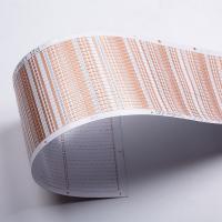
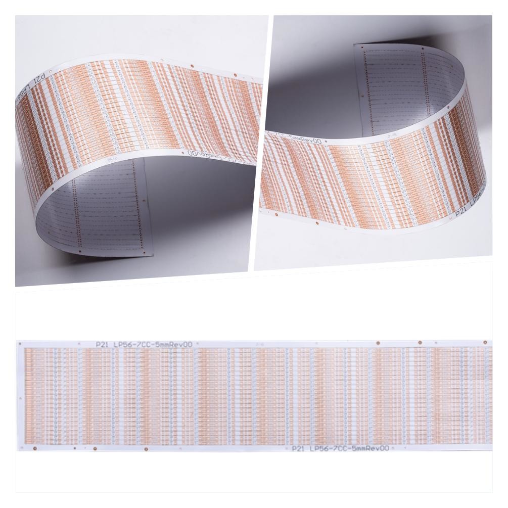
FR4 TG130 Single Sided PCB Flexible Printed Circuit Board 8mil
Single Sided PCB One Sided Flexible Printed Circuit Board Flexible PCB Singple Sided PCB Board Single Sided Board
One sided Flexible Printed Circuit Board
PCB thickness: 0.2~4.0mm(<0.2 mm,>4 mm needs to review) (Board
thickness ≤ 0.6mm,do not apply for HASL surface)
copper thickness of inner and outer base copper: Min 0.3/0.5oz,Max
3oz, advance 4-6oz
Bow and twist: 0.075%
Min. hole size: 0.15mm(<0.15 mm needs to review)
HDI Min drill hole: 0.08-0.10MM
PCB track/gap: 3mil(0.075mm)
PCB outline: Routing/V-CUT/Punching
Solder mask thickness: standard 15-20um; Advanced: 35um
Min solder mask bridge width: green 4mil,other colour 4.8mil
Solder mask filling holes: 0.1-0.5mm
The color of solder mask: green,matt green,blue,matt
blue,black,matt black,yellow,red,white,etc
PCB silkscreen: White, Black and as your request
Peelable mask thickness: 500-1000um
Oxidation film of OSP: 0.2-0.5um
| FPC Technology Capability | |||
| Attribute (All dimensions are mils unless otherwise specified) | Mass Production (Yield≥ 80%,Cpk≥1.33) | Small Amount(Yield≥60%, Key Specification Yield≥80% | Sample |
| FPC(yes/no) | yes | yes | yes |
| Layer count/Structure, Max. | 2 | 4 | 6 |
| Size(L×W), Max. | 550mm*250mm | 550mm*250mm | 700mm*250mm |
| Nominal thickness (mm) | 0.1~0.5 | 0.1~0.5 | 0.1~0.8 |
| Thickness tolerance | ±10%(>0.3mm)/±0.03mm(≤0.3mm) | ±10%(>0.3mm)/±0.03mm(≤0.3mm) | ±10%(>0.3mm)/±0.03mm(≤0.3mm) |
| Surface finish type | ENIGENEPIGOPSI-SilverI-Tin HASLHard Gold | ENIGENEPIGOPSI-SilverI-Tin HASLHard Gold | ENIGENEPIGOPSI-SilverI-Tin HASLHard Gold |
| Soft ENIG(yes/no) | no | no | no |
| Base material type | PI | PI | PILCPTK |
| Coverlay thickness (um) | 28/50/60/80 | 28/50/60/80 | 28/50/60/80 |
| Adhesive thickness (um) | 25/40/50/65 | 25/40/50/65 | 25/40/50/65 |
| Copper thickness, Min./Max. (um) | 12-70 | 12-70 | 12-70 |
| Base material thickness, Min./Max. (um) | 25-75 | 25-75 | 25-100 |
| Mechanical drilled thru-hole size (DHS), Min. | 0.15 | 0.15 | 0.15 |
| Plating aspect ratio, Max. | 3:1 | 3:1 | 5:1 |
| Pad size, Min. | With through hole:0.4mm Without through hole:0.2mm | With through hole:0.4mm Without through hole:0.2mm | With through hole:0.3mm Without through hole:0.2mm |
| Pad size tolerance | 20% | 20% | 10% |
| Pad to pad space, Min. | 4mil | 4mil | 4mil |
| Pad to outline tolerance | ±3mil | ±3mil | ±2mil |
| Pattern location accurancy | ±3mil | ±3mil | ±2mil |
| Pattern location accurancy from top side to bottom | ±3mil | ±3mil | ±2mil |
| Laser via hole diameter/pad, Min. | 4/12mil | 4/10mil | 4/10mil |
| Outerlayer(Hoz+plating) line width/space, Min. | 3/3mil | 3/3mil | 2/2mil |
| Innerlayer(Hoz) line width/space, Min. | 3/3mil | 3/3mil | 2/2mil |
| Inner line width tolerance | ±10% | ±10% | ±10% |
| Outerlayer registration, Min. (Pad diameter = DHS + X) | DHS + 8 | DHS + 8 | DHS + 6 |
| Innerlayer registration, Min. (Pad diameter = DHS + X)(L≤4 layer) | DHS + 10 | DHS + 10 | DHS + 8 |
| Laser via hole pitch, Min. | 0.40mm | 0.40mm | 0.35mm |
| Mechanical hole pitch, Min. | 0.50mm | 0.50mm | 0.40mm |
| Drilled hole position tolerance | ±2mil | ±2mil | ±2mil |
| Hole size tolerance | ±2mil | ±2mil | ±2mil |
| Location accurancy from tooling hole(PTH&NPTH) to pad | ±3mil | ±3mil | ±2mil |
| Location accurancy from tooling hole(PTH&NPTH) to outline | ±3mil | ±3mil | ±2mil |
| Outline size tolerance | ±2mil | ±2mil | ±2mil |
| LPI registration/dam, Min. | 2mil/4mil | 2mil/4mil | 2mil/3mil |
| LPI dam on CVL | 8mil | 8mil | 8mil |
| Coverlay open window/dam | Φ0.5mm/0.3mm | Φ0.5mm/0.3mm | Φ0.3mm/0.2mm |
| Coverlay registration/Resin flow | 4mil | 4mil | 2mil |
| Stifferness material | FR4/PI/Steel | FR4/PI/Steel | FR4/PI/Steel |
| Stifferness dam, Min. | 12mil | 12mil | 8mil |
| Stifferness registration/Resin flow | 8mil/4mil | 8mil/4mil | 4mil/2mil |
| Impedance tolerance | 10% | 10% | 5% |
| Thermal reliability(LPI, FCCL, CVL) | 288°/10s/3times | 288°/10s/3times | 288°/10s/3times |
| Qualified material and structure UL | PI | PI | PI |
FAQ:
Q1:Are you a factory or trade company?
A: Yes, we are the factory, we have independent quick turn
prototype PCB manufacturing & big volume PCB production lines.
Q2:How about your PCB factory production capacity?
A: Our monthly production capacity is 50,000 square meter/month and
5000types/month.
Q3:If we have no PCB file/Gerber file, only have the PCB sample,can
you produce it for me?
A: Yes,we could help you to clone the PCB. Just send the sample PCB
to us, we could clone the PCB design and work out it.
Q4:How will you usually ship the PCB?
A: Usually for small packages, we will ship the boards by
DHL,UPS,FedEx door to door service, we could use your shipping
account to do collection or use our account to ship in DDU (import
duty unpaid) delivery term.
For heavy goods more than 300kg, we may ship your PCB boards by
ship or by air to save freight cost. Of course, if you have your
own forwarder, we may contact them for dealing with your shipment.
Q5:What is your standard lead time for production?
A: Sample/prototype(less than 3sqm):
1-2 Layers: 3 to 5working days (fastest 24hours for quick turn
services)
4-8 Layers: 7~12 working days (fastest 48hours for quick turn
services)
Mass production (less than 200sqm):
1-2 Layers:7 to 12 working days
4-8 Layers:10 to 15 working days


