|
|
[China]

Trade Verify
Address: Shenzhen YingSheng Technology Co., Ltd 805, Tongxin Technology Building, Qiaotou Community, Fuhai Street, Baoan District, Shenzhen
Contact name:Zhou

Shenzhen Yingsheng Technology Co., Ltd. |
|
Verified Suppliers
|
|
|
To ensure that the connection works adequately, materials are
welded or inserted into a blank circuit board and inspected to test
their performance.
A bare PCB consists of a sheet formed by an insulating material,
copper foil, and a coating to protect the copper from corrosion.
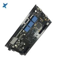
While a PCBA is mounted with all the assembled electronic
components.
Nowadays, almost all components can be surface mounted on circuit
boards. Through-hole technology is still in use but less and less
in PCB assembly.
Part 2: How to Get a Custom PCBA
In this section, we will have a look at how to create a custom
PCBA.
Step1. The first step in designing a custom PCB is in creating a
schematic view.
The required component is placed on a canvas and their pins are
connected with lines that represent the electrical connections. The
components usually are taken from a component library which is a
part of the design software.
There may be multiple variations of the same components depending
upon the type of package being used e.g. dual inline package or a
surface-mounted chip. The packages may seem the same in the
schematic view but are very different in the layout view where the
board is actually designed.
Apart from the components and their electrical connections, power,
and ground signals are also needed. Also, connectors have to be
placed on the PCB to make a place for power and ground. The board
is also required to be connected to external devices such as
potentiometers and LEDs etc.
| YScircuit HDI PCB manufacturing capabilities overview | |
| Feature | capabilities |
| Layer Count | 4-60L |
| Available HDI PCB Technology | 1+N+1 |
| 2+N+2 | |
| 3+N+3 | |
| 4+N+4 | |
| 5+N+5 | |
| Any layer | |
| Thickness | 0.3mm-6mm |
| Minimum line Width and Space | 0.05mm/0.05mm(2mil/2mil) |
| BGA PITCH | 0.35mm |
| Min laser Drilled Size | 0.075mm(3nil) |
| Min mechanical Drilled Size | 0.15mm(6mil) |
| Aspect Ratio for laser hole | 0.9:1 |
| Aspect Ratio for through hole | 16:1 |
| Surface Finish | HASL, Lead free HASL,ENIG,Immersion Tin, OSP, Immersion Silver, Gold Finger, Electroplating Hard Gold, Selective OSP,ENEPIG.etc. |
| Via Fill Option | The via is plated and filled with either conductive or non-conductive epoxy then capped and plated over |
| Copper filled, silver filled | |
| Laser via copper plated shut | |
| Registration | ±4mil |
| Solder Mask | Green, Red, Blue, White, Black, Purple, Matte Black, Matte
green.etc. |
| layer/m² | S<1㎡ | S<3㎡ | S<6㎡ | S<10㎡ | S<13㎡ | S<16㎡ | S<20㎡ | S<30㎡ | S<40㎡ | S<50㎡ | S<65㎡ | S<85㎡ | S<100㎡ |
| 1L | 4wds | 6wds | 7wds | 7wds | 9wds | 9wds | 10wds | 10wds | 10wds | 12wds | 14wds | 15wds | 16wds |
| 2L | 4wds | 6wds | 9wds | 9wds | 11wds | 12wds | 13wds | 13wds | 15wds | 15wds | 15wds | 15wds | 18wds |
| 4L | 6wds | 8wds | 12wds | 12wds | 14wds | 14wds | 14wds | 14wds | 15wds | 20wds | 25wds | 25wds | 28wds |
| 6L | 7wds | 9wds | 13wds | 13wds | 17wds | 18wds | 20wds | 22wds | 24wds | 25wds | 26wds | 28wds | 30wds |
| 8L | 9wds | 12wds | 15wds | 18wds | 20wds | 20wds | 22wds | 24wds | 26wds | 27wds | 28wds | 30wds | 30wds |
| 10L | 10wds | 13wds | 17wds | 18wds | 20wds | 20wds | 22wds | 24wds | 26wds | 27wds | 28wds | 30wds | 30wds |
| 12L | 10wds | 15wds | 17wds | 18wds | 20wds | 20wds | 22wds | 24wds | 26wds | 27wds | 28wds | 30wds | 30wds |
| 14L | 10wds | 16wds | 17wds | 18wds | 20wds | 20wds | 22wds | 24wds | 26wds | 27wds | 28wds | 30wds | 30wds |
| 16L | 10wds | 16wds | 17wds | 18wds | 20wds | 20wds | 22wds | 24wds | 26wds | 27wds | 28wds | 30wds | 30wds |