
|
|
[China]

Trade Verify
Address: Shenzhen YingSheng Technology Co., Ltd 805, Tongxin Technology Building, Qiaotou Community, Fuhai Street, Baoan District, Shenzhen
Contact name:Zhou

Shenzhen Yingsheng Technology Co., Ltd. |
|
Verified Suppliers
|
|
|
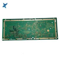
HDI PCB Quick Turn Printed Circuit Boards Double-Sided Multilayer Fr4
What is considered a quick turn in PCB manufacturing?
Quick turn PCBs vary dramatically depending on their complexity, delivery requirements, and volume. Prototypes can generally be delivered extremely quickly, but as variables scale in scope, delivery times
For simple, two-layer constructions, costs can be kept at a minimum and delivered on a very short timeline. As requirements increase, fabrication and production take longer in turn. Keeping these things in mind is critical when considering what a quick turn means in PCB manufacturing.
Multilayer Printed Circuit Board, It is a type of PCB which comes with a combination of single sided PCB and double sided PCB.
It features layers more than double sided PCB.
PCB Sideplating
Sideplating is the metalization of the board edge in the PCB filed.
Edge plating, Border plated, plated contour, side metal, these words can also be used to describe the same function.
Half-cut Castellated Holes
Castellations are plated through holes or vias located in the edges of a printed circuit board.
Are indentations created in the form of semi-plated holes on the edges of the PCB boards.
These half holes serve as pads intended to create a link between the module board and the board that it will be soldered onto.
Parameters
| layer/m² | S<1㎡ | S<3㎡ | S<6㎡ | S<10㎡ | S<13㎡ | S<16㎡ | S<20㎡ | S<30㎡ | S<40㎡ | S<50㎡ | S<65㎡ | S<85㎡ | S<100㎡ |
| 1L | 4wds | 6wds | 7wds | 7wds | 9wds | 9wds | 10wds | 10wds | 10wds | 12wds | 14wds | 15wds | 16wds |
| 2L | 4wds | 6wds | 9wds | 9wds | 11wds | 12wds | 13wds | 13wds | 15wds | 15wds | 15wds | 15wds | 18wds |
| 4L | 6wds | 8wds | 12wds | 12wds | 14wds | 14wds | 14wds | 14wds | 15wds | 20wds | 25wds | 25wds | 28wds |
| 6L | 7wds | 9wds | 13wds | 13wds | 17wds | 18wds | 20wds | 22wds | 24wds | 25wds | 26wds | 28wds | 30wds |
| 8L | 9wds | 12wds | 15wds | 18wds | 20wds | 20wds | 22wds | 24wds | 26wds | 27wds | 28wds | 30wds | 30wds |
| 10L | 10wds | 13wds | 17wds | 18wds | 20wds | 20wds | 22wds | 24wds | 26wds | 27wds | 28wds | 30wds | 30wds |
| 12L | 10wds | 15wds | 17wds | 18wds | 20wds | 20wds | 22wds | 24wds | 26wds | 27wds | 28wds | 30wds | 30wds |
| 14L | 10wds | 16wds | 17wds | 18wds | 20wds | 20wds | 22wds | 24wds | 26wds | 27wds | 28wds | 30wds | 30wds |
| 16L | 10wds | 16wds | 17wds | 18wds | 20wds | 20wds | 22wds | 24wds | 26wds | 27wds | 28wds | 30wds | 30wds |
| 0-0.5m2 | 0.5-1m2 | 1-3m2 | 3-5m2 | 5-10m2 | |
| 1-2L | 24H | 24H | 3wds | 4wds | 5wds |
| 4L | 24H | 48H | 4wds | 5wds | 6wds |
| 6L | 48H | 48H | 4wds | 6wds | 6wds |
| 8L | 48H | 36H | 5wds | 6wds | 8wds |
| Technical index | Mass Batch | Small batch | Sample | ||
| Base Material | FR4 | Normal Tg | Shengyi S1141,KB6160(not suitable for lead free process) | ||
| Middle Tg | For HDI, multi layers: SY S1000H,ITEQIT158.TU-662 | ||||
| High Tg | For thick copper, high layer: SY S1000-2;ITEQIT180A;ISOLA:FR408R;370HR;TU-752; | ||||
| Halogen Free | Middle Tg:SYS1150G.H160HF;high Tg: SYS1165 | ||||
| High CTI | CTl≥600 SY S1600 | ||||
| High Frequency | Rogers,Arion,Taconic,SY SCGA-500.S7136 | ||||
| High Speed | SYS7439,TU-862HF.TU-872SLK;ISOLA:l-Speed.1-Tera@MT40; | ||||
| Flex Materia | Base | Glue-free:Dupont AK XingyangW-type,Panosonic RF-775; | |||
| Coverlay | SY SF305C.Xingyang O-type | ||||
| Special PP | No flow PP:VT-447LF.Taiguang 370BL Arion 49N | ||||
| Ceramic filled adhesive sheetRogers4450F | |||||
| PTFE adhesive sheetArion6700.Taconic FR-27/FR-28 | |||||
| Double-sided coating PExingyang N-1010TF-mb | |||||
| Metal Base | Berguist Al-base, chaosun Al-base,copperbase | ||||
| Special | High heat resistance rigidity Pl: TenghuiVT-901.Arion85N.SY S260(Tg250) | ||||
| High thermal conductivty material: 92ML | |||||
| Pure ceramic matenal: alumna ceramic.Aluminum nitride ceramics | |||||
| BT material: Taiwan Nanya NGP-200WT | |||||
| Layers | FR4 | 20 | 36 | 48 | |
| Rigid8Flex/(Flex) | 16(6) | 16(6) | 24(6) | ||
| High Frequency Mixed Lamination | 12 | 12 | 20 | ||
| 100% PTFE | 6 | 6 | 10 | ||
| HDI | 4 steps | 4 steps | 4 steps | ||
| Technical lndex | Mass Batch | Small Batch | Sample | ||
| Delivery Size | Max(mm) | 1200*560 | 1200*560 | 1200*560 | |
| (mm) | Min(mm) | 20*20 | 10"10 | 5*10 | |
| Finish board thickness | Max(mm) | 10 | |||
| Min(mm) | 0.3 | ||||
| Width/Gap | Inner(mil) | 0.5OZ base cooper: 3/3 1.0OZ base copper: 4/42.0OZ base copoer: 516 | |||
| 3.0OZ base cooper: 7/9 4.0OZ base copper: 8/12 5.0OZ base copper: 10/15 | |||||
| 6.0OZ basecooper: 12/18 10OZ basecopper: 18/24 12OZ base copper: 20/28 | |||||
| Outer (mil) | 1/3OZ base copper: 3/3 0.5OZ base copper: 4/4 1.0OZ base copper: 5/5 | ||||
| 2.0OZ base cooper: 6/8 3.0OZ base copper: 7/10 4.0OZ base copper: 8/13 | |||||
| 5.0OZ base cooper: 10/16 6.0OZ base copper: 12/18 10OZ base copper:18/24 | |||||
| 12OZ base copper: 20/28150Z base copper: 24/32 | |||||
| Line Width Tolerance | >5.0 mil | ±20% | ±20% | ±1.0mil | |
| ≤5.0 mil | ±1.0mil | ±1.0mil | ±1.0mil | ||
| Drilling | Min laser(mm) | 0.1 | 0.1 | 0.1 | |
| Min CNC(mm) | 0.2 | 0.15 | 0.15 | ||
| Max CNC drill bit (mm) | 6.5 | 6.5 | 6.5 | ||
| Min Half Hole(mm) | 0.5 | 0.4 | 0.4 | ||
| PTH Hole(mm) | Normal | ±0.1 | ±0.075 | ±0.075 | |
| Pressing Hole | ±0.05 | ±0.05 | ±0.05 | ||
| Hole Angle(conical) | Width of upper diameters≤6.5mm:800,900,1000,1100:Width of upper diameters≤65mm:900; | ||||
| Frecision of Depth-control Drilling (mm) | ±0.10 | ±0.075 | ±0.05 | ||
| Number of blind CNC holes of one sidd | ≤2 | ≤3 | ≤4 | ||
| Minimum via hole spacing (different network, military, medical, automobile )mm | 0.5 | 0.45 | 0.4 | ||
| Minimum via spacing(different network, general industrial control and consumer electronic ) mm | 0.4 | 0.35 | 0.3 | ||
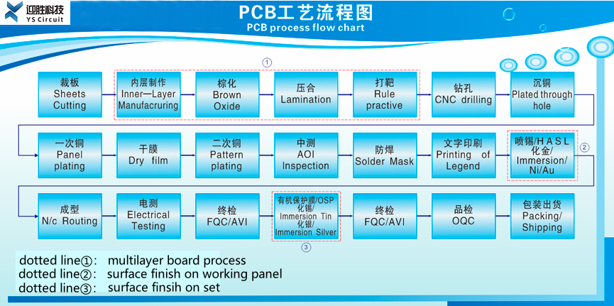
YScircuit Print Circuit Boards Production Process
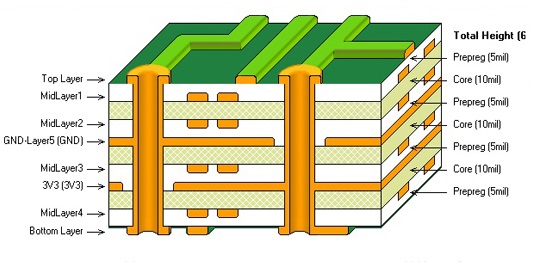
PCB Stack UP


FQA
1. What is hard gold in PCB?
The Hard Gold surface finish, also known as Hard Electrolytic Gold, is composed of a layer of gold with added hardeners for increased durability, plated over a barrier coat of nickel using an electrolytic process.
2. What is hard gold plating?
Hard gold plating is a gold electrodeposit that has been alloyed
with another element to alter the grain structure of the gold to
achieve a harder deposit with a more refined grain structure.
The most common alloying elements used in hard gold plating are cobalt, nickel or iron.
3. What is the difference between Enig and hard gold?
ENIG plating is much softer than hard gold plating.
Grain sizes are about 60 times larger with ENIG plating, and hardness runs between 20 and 100 HK25.
ENIG plating holds up well at only 35 grams of contact force or less, and ENIG plating typically lasts for fewer cycles than hard plating.
A popular trend among manufacturers is board-to-board soldering.
This technique allows companies to produce integrated modules (often containing dozens of parts) on a single board that can be built into another assembly during production.
One easy way to produce a PCB that is destined to be mounted to another PCB is to create castellated mounting holes.
These are also known as "castellated vias" or "castellations."
| layer/m² | S<1㎡ | S<3㎡ | S<6㎡ | S<10㎡ | S<13㎡ | S<16㎡ | S<20㎡ | S<30㎡ | S<40㎡ | S<50㎡ | S<65㎡ | S<85㎡ | S<100㎡ |
| 1L | 4wds | 6wds | 7wds | 7wds | 9wds | 9wds | 10wds | 10wds | 10wds | 12wds | 14wds | 15wds | 16wds |
| 2L | 4wds | 6wds | 9wds | 9wds | 11wds | 12wds | 13wds | 13wds | 15wds | 15wds | 15wds | 15wds | 18wds |
| 4L | 6wds | 8wds | 12wds | 12wds | 14wds | 14wds | 14wds | 14wds | 15wds | 20wds | 25wds | 25wds | 28wds |
| 6L | 7wds | 9wds | 13wds | 13wds | 17wds | 18wds | 20wds | 22wds | 24wds | 25wds | 26wds | 28wds | 30wds |
| 8L | 9wds | 12wds | 15wds | 18wds | 20wds | 20wds | 22wds | 24wds | 26wds | 27wds | 28wds | 30wds | 30wds |
| 10L | 10wds | 13wds | 17wds | 18wds | 20wds | 20wds | 22wds | 24wds | 26wds | 27wds | 28wds | 30wds | 30wds |
| 12L | 10wds | 15wds | 17wds | 18wds | 20wds | 20wds | 22wds | 24wds | 26wds | 27wds | 28wds | 30wds | 30wds |
| 14L | 10wds | 16wds | 17wds | 18wds | 20wds | 20wds | 22wds | 24wds | 26wds | 27wds | 28wds | 30wds | 30wds |
| 16L | 10wds | 16wds | 17wds | 18wds | 20wds | 20wds | 22wds | 24wds | 26wds | 27wds | 28wds | 30wds | 30wds |
| 0-0.5m2 | 0.5-1m2 | 1-3m2 | 3-5m2 | 5-10m2 | |
| 1-2L | 24H | 24H | 3wds | 4wds | 5wds |
| 4L | 24H | 48H | 4wds | 5wds | 6wds |
| 6L | 48H | 48H | 4wds | 6wds | 6wds |
| 8L | 48H | 36H | 5wds | 6wds | 8wds |


