
|
|
[China]

Trade Verify
Address: 3602, Unit 1, Building 2, Phase 3, Longhu Zichen Xiangsong, Huazhaobi Xiaheng Street, Jinniu District, Chengdu, China
Contact name:Sia Li

Chengdu Cesgate Technology Co., Ltd |
|
Verified Suppliers
|
|
|
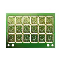
Bom In D365 RF PCB Board Altium Designer 17 Bom Build Of Materials Active Element
Metal Core PCB Manufacturing Customized PCB Rigid Printed Circuit Boards
CESGATE with customers to provide them with the highest-quality RF PCB board and PCBA electronic manufacturing services to achieve their goals. Our flexibility is in meeting customer requirements and our superior customer service. We help companies introduce their new products to market in the fastest time possible by providing high quality, quick-turn assembly.We provide one-stop electronic manufacturing service to help you qualify your designs and provide quality samples to your customers.
The reason why PCB can be used more and more widely is because it has many unique advantages, which are summarized as follows.
1 can be high density. For decades, with the improvement of
integrated circuit integration and the advancement of mounting
technology, the high density of printed boards has been developed.
2 High reliability. Through a series of inspections, tests and
burn-in tests, the RF PCB board can work reliably for a
long time (usually 20 years).
3 Designability. For RF PCB board performance (electrical,
physical, chemical, mechanical, etc.) requirements, printed board
design can be achieved through design standardization,
standardization, etc., with short time and high efficiency.
4 Manufacturability. With modern management, standardized,
large-scale (quantitative) and automated production can be carried
out to ensure the consistency of product quality.
5 Testability. We have established relatively complete test
methods, test standards, various test equipment and instruments to
test and evaluate the eligibility and service life of PCB products.
Industrial application
High-power industrial applications of PCBs are common. These
electronic components control the mechanisms used in factories and
manufacturing facilities and must withstand the harsh conditions
commonly found in industrial installations. This can include
anything including harsh chemicals, vibrating machinery and rough
handling.
In such a rapidly challenging environment, industry standards are
equally stringent. Currently, thick copper PCBs (much thicker than
standard ounce PCBs) are often seen in other applications. This PCB
is helpful for high current industrial applications and battery
chargers.
1. Industrial Equipment: Many drills and presses used in
manufacturing operate using PCB-controlled electronics.
2. Measuring Equipment: Equipment used to measure and control
pressure, temperature and other variables in industrial
manufacturing processes.
3. Power equipment: DC-AC power inverter, solar cogeneration
equipment and other power control equipment.
PCB Capacities and Technical Specification
| NO. | Items | Capabilities |
| 1 | Layers | 2-68L |
| 2 | Maximum machining size | 600mm*1200mm |
| 3 | Board thickness | 0.2mm-6.5mm |
| 4 | Copper thickness | 0.5oz-28oz |
| 5 | Min trace/space | 2.0mil/2.0mil |
| 6 | Minimum finished aperture | 0. 10mm |
| 7 | Maximum thickness to diameter ratio | 15:1 |
| 8 | Via treatment | Via, blind&buried via, via in pad, Copper in via … |
| 9 | Surface finish/treatment | HASL/HASL lead free, Chemical tin, Chemical Gold, Immersion gold Inmersion Silver/Gold, Osp, Gold Plating |
| 10 | Base Material | FR408 FR408HR, PCL-370HR;IT180A, Megtron 6(Panasonic);Rogers4350, Rogers4003, RO3003, Rogers/Taconic/Arlon/Nelco laminate with FR-4 material(including partial Ro4350B hybrid laminating with FR-4) |
| 11 | Solder mask color | Green.Black.Red.Yellow.White.Blue.Purple.Matte Green. Matte Black |
| 12 | Testing Service | AOI, X-Ray, Flying-Probe, Function Test, First Article Tester |
| 13 | Profiling Punching | Routing,V-CUT,Beveling |
| 14 | Bow&twist | ≤0.5% |
| 15 | HDI type | 1+n+1,2+n+2,3+n+3 |
| 16 | Min mechanical aperture | 0.1mm |
| 17 | Min laser aperture | 0.075mm |
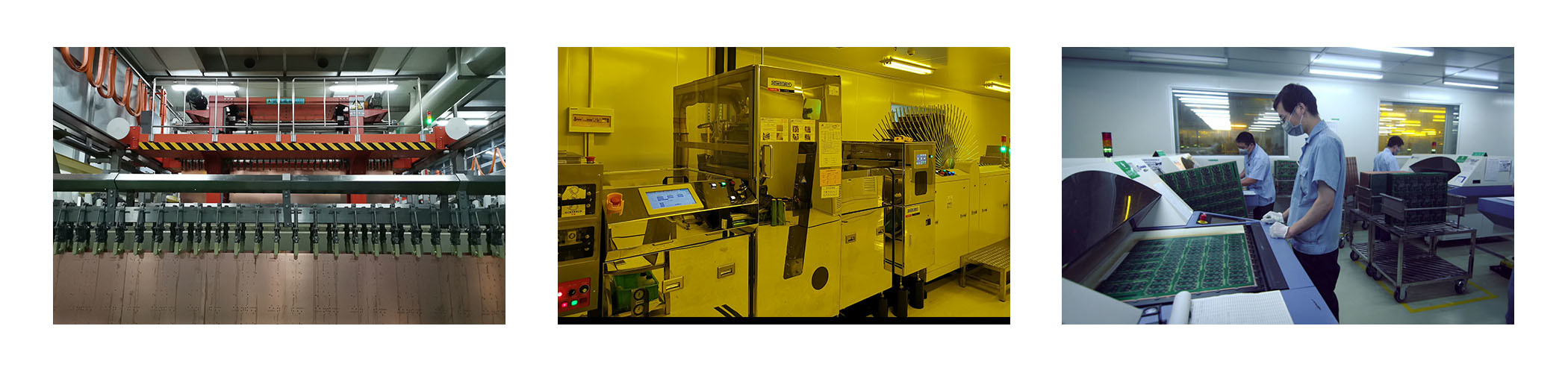
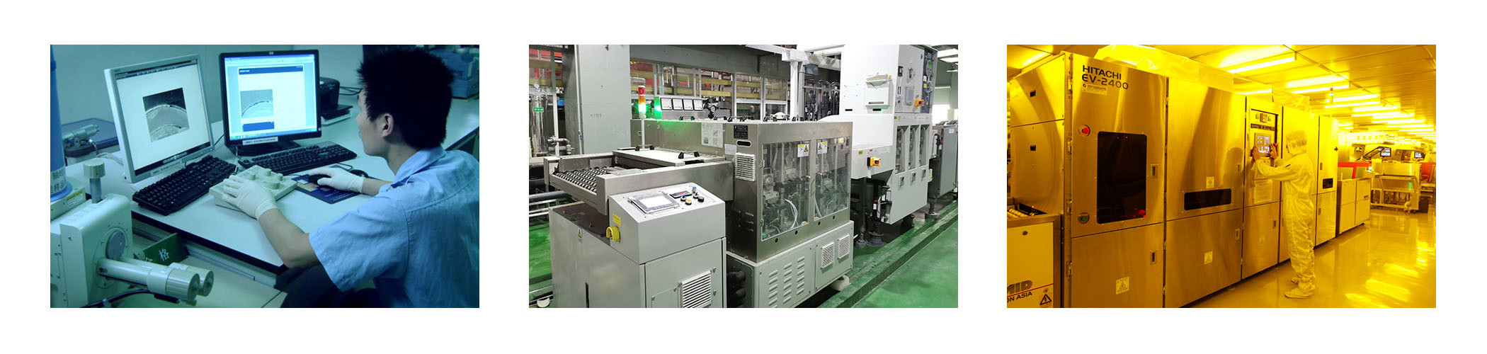
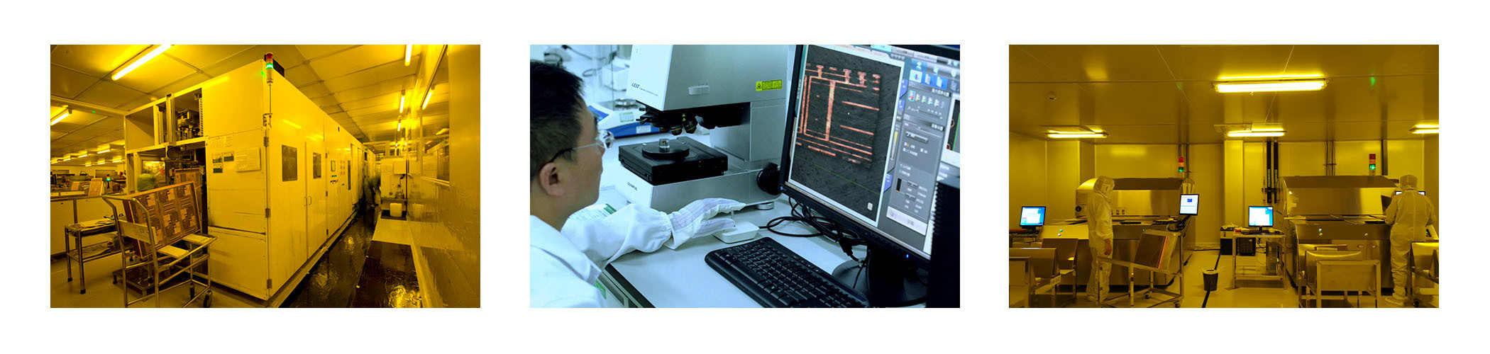
Advanced PCB Manufacturing and PCB Assembly Equipment
CESGATE has imported the advanced machinery from US,Japan,German and Israel to improve our production and technical ability.We have set a great example the RF PCB Board field of flying probe testing,buried and blind via and special controlled impedance.We have a highly developed R&D division which has helped our factory successfully produce mechanical micro via,high density impedance and HDI.


FAQ:
| Q: Do you support fast proofing? CESGATE: Yes, we support fast proofing within 3-7 days. |
| Q: What is your inspection policy? How do you control the quality? CESGATE: In order to ensure the quality of PCB products, flying probe inspection is usually used; electrical fixtures, automatic optical inspection (AOI), BGA parts x-ray inspection, first article inspection ( FAI) etc. |
| Q: How about the shipping cost? CESGATE: The Shipping cost depends on the destination, the weight and volume of the goods as well as the quotation of DHL/FEDEX/ freight forwarder at that time. You can inform us of the transportation way you need before placing an order. |
| Q: Can we inspect quality during production? CESGATE: Yes, we are open and transparent on each production process with nothing to hide. We welcome customer inspect our production process and check in house. |


