
|
|
[China]

Trade Verify
Address: 3602, Unit 1, Building 2, Phase 3, Longhu Zichen Xiangsong, Huazhaobi Xiaheng Street, Jinniu District, Chengdu, China
Contact name:Sia Li

Chengdu Cesgate Technology Co., Ltd |
|
Verified Suppliers
|

|
|
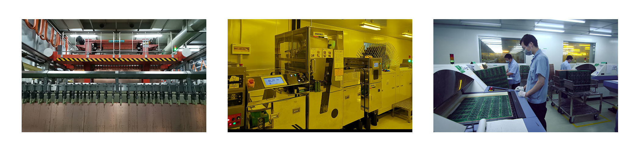
AOI machines Flying Probe Fabrication PCB Prototype Service High Tg FR4
PCB surface treatment
Since the copper surface of the PCB Prototype Service is easily
oxidized in the environment, it must be reprocessed and covered
with a layer of coating on the exposed area that is not covered
with solder mask ink to protect the process from oxidation. In
response to various subsequent processing needs, various surface
treatment processing methods with different materials, prices and
different degrees of protection have been developed.
Common PCB Prototype Service surface treatments include the following:
Bare copper plate, spray tin plate, lead-free spray tin plate, chemical gold plate, electroplating gold, chemical silver plate, OSP plate.
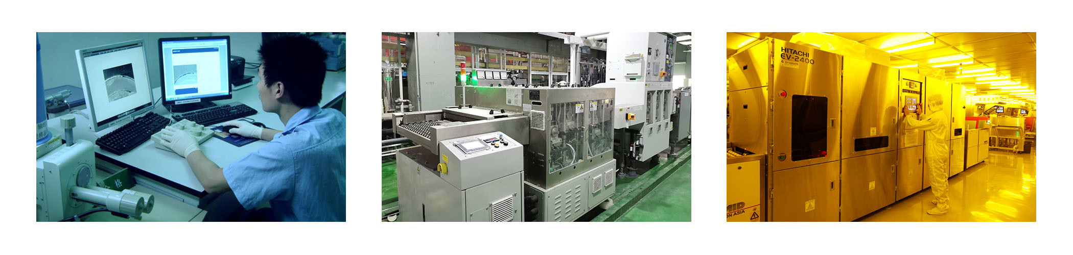
PCB Prototype Service Process - Introduction to HDI
HDI (High Density Interconnect): High-density interconnection
technology, mainly using micro-blind / buried vias (blind / buried
vias), a technology that makes PCB circuit board circuit
distribution density higher. The advantage is that it can greatly
increase the usable area of the PCB circuit board, making the
product as miniaturized as possible. However, due to the increase
in line distribution density, it is impossible to use traditional
drilling methods to drill through holes, and some of the via holes
must be drilled with laser drilling to form blind holes, or
cooperate with inner-layer buried vias to interconnect.
Generally speaking, HDI circuit boards use the build-up method (Build Up), first do or press the inner layers, laser drilling and electroplating on the outer layer are completed, and then the outer layer is covered with an insulating layer (prepreg). ) and copper foil, and then repeat the outer layer circuit making, or continue to laser drill, and stack the layers outward one at a time.
Generally, the diameter of the laser drilling hole is designed to be 3 ~ 4 mil (about 0.076 ~ 0.1 mm), and the insulation thickness between each laser drilling layer is about 3 mil. Due to the use of laser drilling many times, the key to the quality of the HDI circuit board is the hole pattern after laser drilling and whether the hole can be evenly filled after the subsequent electroplating and filling.
The following are examples of HDI board types. The pink holes in the picture are blind holes, which are made by laser drilling, and the diameter is usually 3 to 4 mil; the yellow holes are buried holes, which are made by mechanical drilling, and the diameter is at least 6 mil (0.15 mm).
PCB Prototype Service Capacities and Technical Specification
| NO. | Items | Capabilities |
| 1 | Layers | 2-68L |
| 2 | Maximum machining size | 600mm*1200mm |
| 3 | Board thickness | 0.2mm-6.5mm |
| 4 | Copper thickness | 0.5oz-28oz |
| 5 | Min trace/space | 2.0mil/2.0mil |
| 6 | Minimum finished aperture | 0. 10mm |
| 7 | Maximum thickness to diameter ratio | 15:1 |
| 8 | Via treatment | Via, blind&buried via, via in pad, Copper in via … |
| 9 | Surface finish/treatment | HASL/HASL lead free, Chemical tin, Chemical Gold, Immersion gold Inmersion Silver/Gold, Osp, Gold Plating |
| 10 | Base Material | FR408 FR408HR, PCL-370HR;IT180A, Megtron 6(Panasonic);Rogers4350, Rogers4003, RO3003, Rogers/Taconic/Arlon/Nelco laminate with FR-4 material(including partial Ro4350B hybrid laminating with FR-4) |
| 11 | Solder mask color | Green.Black.Red.Yellow.White.Blue.Purple.Matte Green. Matte Black |
| 12 | Testing Service | AOI, X-Ray, Flying-Probe, Function Test, First Article Tester |
| 13 | Profiling Punching | Routing,V-CUT,Beveling |
| 14 | Bow&twist | ≤0.5% |
| 15 | HDI type | 1+n+1,2+n+2,3+n+3 |
| 16 | Min mechanical aperture | 0.1mm |
| 17 | Min laser aperture | 0.075mm |
Welcome to Chengdu Cesgate Technology Co., Ltd
We can provide one-stop service:
PCB circuit boards+Assembly
E-test.
Electronic components purchasing.
PCB assembly: available on SMT, BGA, DIP.
PCBA function test.
Enclosure assembly.


FAQ
| Q: Do you support fast proofing? CESGATE: Yes, we support fast proofing within 3-7 days. |
| Q: Are my files safe? CEGSATE: Your files are kept very safe, and we are protecting intellectual property for our clients throughout the process. All files provided by customers are never shared with any third party. |
| Q: MOQ? CESGATE: There is no MOQ in POE. We are able to flexibly handle small and large batches. |
| Q: Do you have any other services? CESGATE: We mainly focus on the procurement services of PCB + assembly + components. In addition, we can also provide programming, testing, cable, housing assembly services. |
| Q: What is your inspection policy? How do you control the quality? CESGATE: In order to ensure the quality of PCB products, flying probe inspection is usually used; electrical fixtures, automatic optical inspection (AOI), BGA parts x-ray inspection, first article inspection ( FAI) etc. |
| Q: What service do you have? CESGATE: We provide turnkey solution including RD, PCB fabrication, SMT, final assembly,testing and other value-added service. |
| Q: What are the main products of your PCB/PCBA services? CESGATE: Our PCB/PCBA services are mainly for the industries including Medical, Automotive, Energy, Metering/Measurements, Consumer Electronics. |
| Q: Is CESGATE a factory or trade company? CESGATE: CESGATE is a factory with PCB factory located in Senzhen and SMT assembly factories in both Shenzhen and Chengdu. |


