
|
|
[China]

Trade Verify
Address: 3602, Unit 1, Building 2, Phase 3, Longhu Zichen Xiangsong, Huazhaobi Xiaheng Street, Jinniu District, Chengdu, China
Contact name:Sia Li

Chengdu Cesgate Technology Co., Ltd |
|
Verified Suppliers
|

|
|
Circuit Board Resistors Digikey Pcb Assembly HDI PCB Flat Bill Of Materials
Introduction to our PCBs
PCB Process - Introduction to HDI
HDI (High Density Interconnect): High-density interconnection
technology, mainly using micro-blind / buried vias (blind / buried
vias), a technology that makes HDI PCB circuit board circuit
distribution density higher. The advantage is that it can greatly
increase the usable area of the HDI PCB circuit board,
making the product as miniaturized as possible. However, due to the
increase in line distribution density, it is impossible to use
traditional drilling methods to drill through holes, and some of
the via holes must be drilled with laser drilling to form blind
holes, or cooperate with inner-layer buried vias to interconnect.
Generally speaking, HDI PCB use the build-up method (Build Up), first do or press the inner layers, laser drilling and electroplating on the outer layer are completed, and then the outer layer is covered with an insulating layer (prepreg). ) and copper foil, and then repeat the outer layer circuit making, or continue to laser drill, and stack the layers outward one at a time.
The following are examples of HDI board types. The pink holes in the picture are blind holes, which are made by laser drilling, and the diameter is usually 3 to 4 mil; the yellow holes are buried holes, which are made by mechanical drilling, and the diameter is at least 6 mil (0.15 mm).
Aerospace applications
Like automotive applications, aerospace applications of PCBs
require extreme precision and durability. Jets and rockets often
experience a lot of turbulence in the atmosphere, which means that
ordinary rigid PCBs can be stressed enough to be damaged in the
process. To solve this problem, most aerospace manufacturers use
flexible PCBs that, in addition to being resistant to vibration
damage, are lightweight and small.
In addition to being durable, aerospace PCBs must be very
high-functioning and precise, manufactured to the best of their
ability to avoid technical issues. Since the electronics used in
aerospace technology are critical to the safety of vehicles and
their crews, it is critical that they function flawlessly.
Some of the more common aerospace applications for PCBs include:
1. Monitoring equipment: Instrumentation, including accelerometers,
pressure sensors, microphones, and torque and force sensors All use
PCBs as part of their basic functions. These products are used in
the engines and cockpits of aircraft and rockets to monitor vehicle
functions and communicate with ground control systems.
2. Test Equipment: In addition to its function as an aircraft, PCBs
are involved in the development and testing of aircraft. Test
equipment that collects data during structural, vibration, and
flight testing uses a PCB as its core. This data can be used to
develop more efficient, efficient and safer aircraft.
PCB Capacities and Technical Specification
| NO. | Items | Capabilities |
| 1 | Layers | 2-68L |
| 2 | Maximum machining size | 600mm*1200mm |
| 3 | Board thickness | 0.2mm-6.5mm |
| 4 | Copper thickness | 0.5oz-28oz |
| 5 | Min trace/space | 2.0mil/2.0mil |
| 6 | Minimum finished aperture | 0. 10mm |
| 7 | Maximum thickness to diameter ratio | 15:1 |
| 8 | Via treatment | Via, blind&buried via, via in pad, Copper in via … |
| 9 | Surface finish/treatment | HASL/HASL lead free, Chemical tin, Chemical Gold, Immersion gold Inmersion Silver/Gold, Osp, Gold Plating |
| 10 | Base Material | FR408 FR408HR, PCL-370HR;IT180A, Megtron 6(Panasonic);Rogers4350, Rogers4003, RO3003, Rogers/Taconic/Arlon/Nelco laminate with FR-4 material(including partial Ro4350B hybrid laminating with FR-4) |
| 11 | Solder mask color | Green.Black.Red.Yellow.White.Blue.Purple.Matte Green. Matte Black |
| 12 | Testing Service | AOI, X-Ray, Flying-Probe, Function Test, First Article Tester |
| 13 | Profiling Punching | Routing,V-CUT,Beveling |
| 14 | Bow&twist | ≤0.5% |
| 15 | HDI type | 1+n+1,2+n+2,3+n+3 |
| 16 | Min mechanical aperture | 0.1mm |
| 17 | Min laser aperture | 0.075mm |
Company Introduction
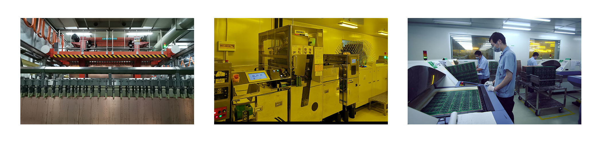
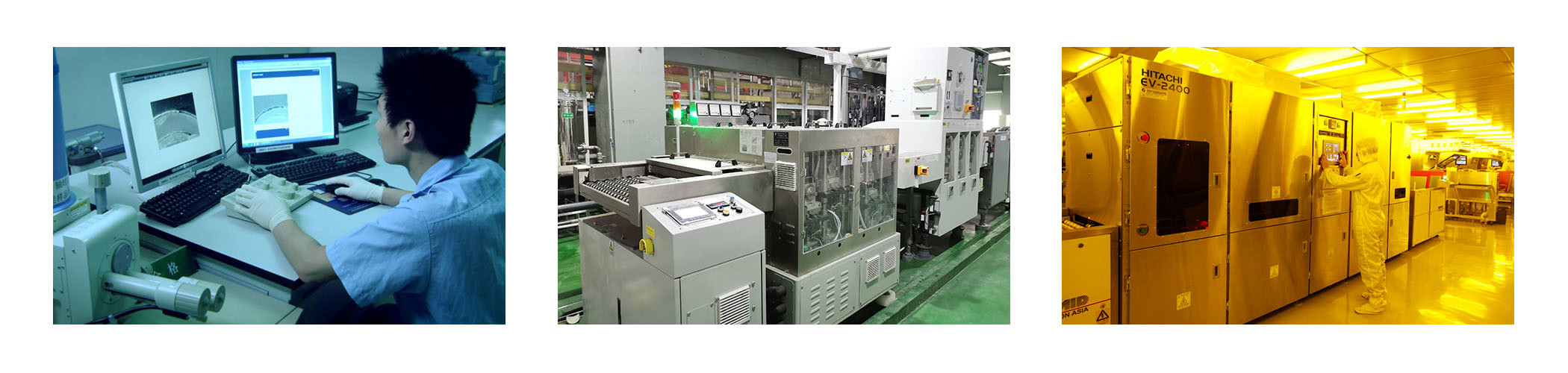
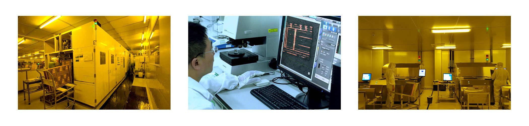
Chengdu Cesgate Technology Co., Ltd. is a high-tech company specializing in providing complete electronic solutions for domestic and foreign customers. We specialize in PCB&PCBA processing/ODM/OEM orders. After 12 years of development, we provide a full range of Electronic Manufacturing Services (EMS) for industrial control, automotive industry, medical applications, telecommunications, military and commercial products with rich experience and professional professionalism. Our services include: Printed Circuit Board Design & Layout, PCB Manufacturing, PCB Assembly & Assembly, Test & System Integration.CESGATE is the professional PCB and PCBA Manufacturer, can provide one-stop service from PCB/PCBA Design, PCB/PCBA Clone, PCB manufacturing, Components sourcing, PCB Assembly, and fully product assembly and test. We have got certification of ISO 9001, ISO 13485 and UL. Our capacity including: 1-32 layers FR4 PCB board manufacturing, 1-12 layers Flexible PCB manufacturing, Aluminum PCB and Ceramic PCB manufacturing, can finish about 324000pcs PCBA per months.


FAQ
| Q: The Wire Bonding process is required when the circuit board is
printed. What should I pay attention to when making the circuit
board? CESGATE: When making circuit boards, the surface treatment options are mostly "nickel palladium gold ENEPIG" or "chemical gold ENIG". If the Al aluminum wire is used, the gold thickness is recommended to be 3μ”~5μ”, but if the Au gold wire is used, the gold thickness should preferably be more than 5μ”. |
| Q: What does CESGATE need for a customized PCB order? CESGATE: When you place a PCB order, the customers need to provide Gerber or pcb file. If you do not have the file in the correct format, you can send all the details related to the products. |
| Q: How can we ensure our information should not let third party to
see our design? CESGATE: We are willing to sign NDA effect by customer side local law and promising to keep customers data in high confidential level. |
| Q: Which express companies do you cooperate with? CESGATE: We cooperate with express companies, including DHL, FedEX, UPS, TNT and EMS. And we also have our own freight forwarders, with lower shipping fees. |
Q: What are the common substrates of CESGATE? |


