
|
|
[China]

Trade Verify
Address: 3602, Unit 1, Building 2, Phase 3, Longhu Zichen Xiangsong, Huazhaobi Xiaheng Street, Jinniu District, Chengdu, China
Contact name:Sia Li

Chengdu Cesgate Technology Co., Ltd |
|
Verified Suppliers
|
|
|
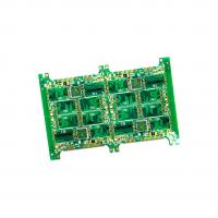
Bldc Fan Circuit Board Smt Control Board PCB Prototype Service Sap Pm Bom
CESGATE Offering
1. 7/24 Sales and technical support
2. Felxible payment methods and negotiable payment terms
3. Both samples and bulk orders are supported
4. More than 10 years overseas export experience, flexible handling
of transportation and customs clearance issues
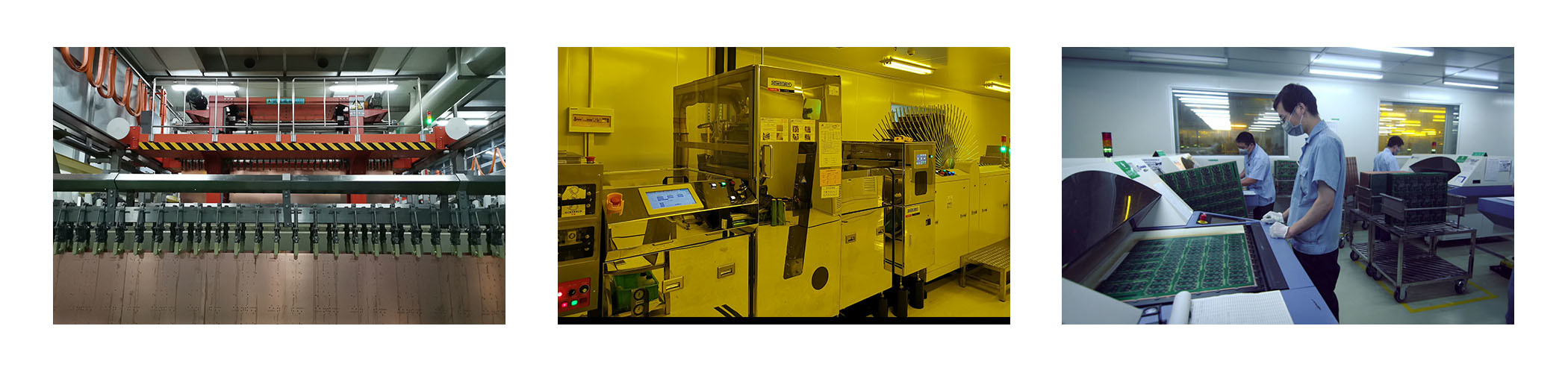
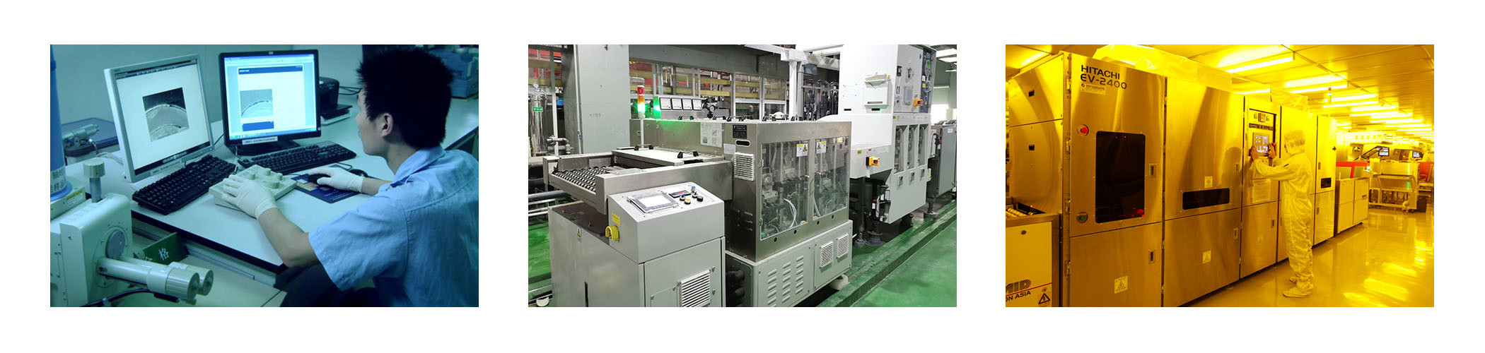
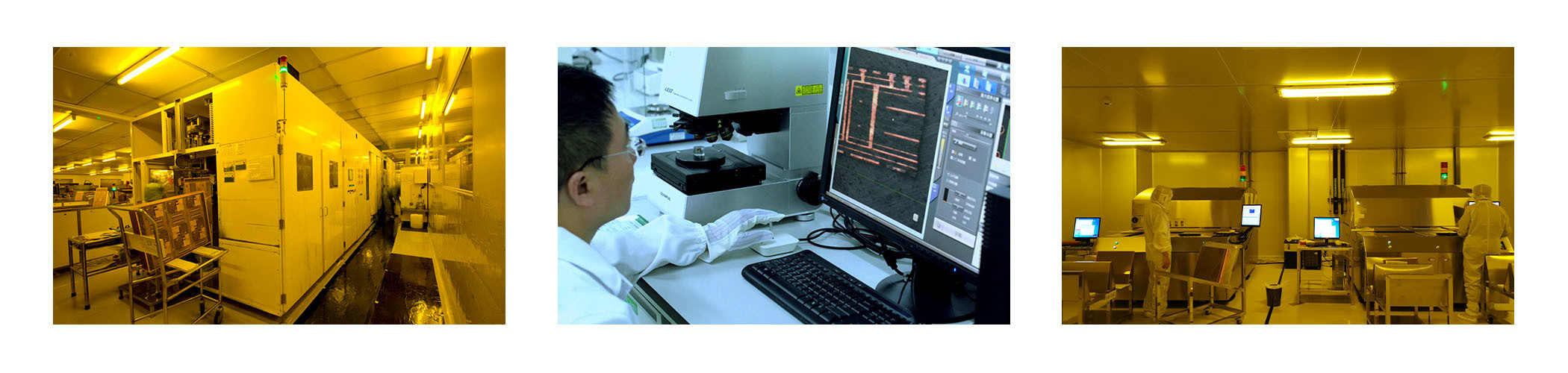
PCB prototype service Capacities and Technical Specification
| NO. | Items | Capabilities |
| 1 | Layers | 2-68L |
| 2 | Maximum machining size | 600mm*1200mm |
| 3 | Board thickness | 0.2mm-6.5mm |
| 4 | Copper thickness | 0.5oz-28oz |
| 5 | Min trace/space | 2.0mil/2.0mil |
| 6 | Minimum finished aperture | 0. 10mm |
| 7 | Maximum thickness to diameter ratio | 15:1 |
| 8 | Via treatment | Via, blind&buried via, via in pad, Copper in via … |
| 9 | Surface finish/treatment | HASL/HASL lead free, Chemical tin, Chemical Gold, Immersion gold Inmersion Silver/Gold, Osp, Gold Plating |
| 10 | Base Material | FR408 FR408HR, PCL-370HR;IT180A, Megtron 6(Panasonic);Rogers4350, Rogers4003, RO3003, Rogers/Taconic/Arlon/Nelco laminate with FR-4 material(including partial Ro4350B hybrid laminating with FR-4) |
| 11 | Solder mask color | Green.Black.Red.Yellow.White.Blue.Purple.Matte Green. Matte Black |
| 12 | Testing Service | AOI, X-Ray, Flying-Probe, Function Test, First Article Tester |
| 13 | Profiling Punching | Routing,V-CUT,Beveling |
| 14 | Bow&twist | ≤0.5% |
| 15 | HDI type | 1+n+1,2+n+2,3+n+3 |
| 16 | Min mechanical aperture | 0.1mm |
| 17 | Min laser aperture | 0.075mm |
PCBA Capabilities
Briefly Introduce Our Strength
1. Can reduce PCB cost. When the prototype PCB service density increases beyond eight layers, it is manufactured by
HDI and its cost will be lower than the traditional complex
pressing process.
2. Increase circuit density, interconnection of traditional circuit
boards and parts
3. Promote the use of advanced building techniques
4. Has better electrical performance and signal accuracy
5. Better reliability
6, can improve thermal performance
7. Can improve RFI/EMI/ESD (RFI/EMI/ESD)
8. Improve design efficiency
Application
Printed circuit boards (PCBs) are indispensable accessories in modern electronic devices. Printed circuit boards are used in all electronic equipment, whether it is large machinery or personal computers, communication base stations or mobile phones, household appliances or electronic toys. .Printed circuit boards are mainly composed of insulating substrates and conductors, which play the role of support, interconnection and part of circuit elements in electronic equipment. Electronic components such as integrated circuits, resistors, capacitors, etc. cannot function as a single entity. They only work as a whole if they have a firm foothold on the prototype PCB service and there are conductive junctions connecting them. Prototype PCB serviceThe printed circuit board is the skeleton that supports the components and is the conduit for connecting electrical signals. In addition, some printed circuit boards have components such as resistors, capacitors, inductors, etc., which become functional circuits and play the role of trachea.


FAQ
Q: What are the common substrates of CESGATE? |
| Q: What is the difference between the HDI board and the general
circuit board? CESGATE: Most of HDI use laser to form holes, while general circuit boards only use mechanical drilling, and HDI boards are manufactured by the build-up method (Build Up), so more layers will be added, while general circuit boards are only added once. |
| Q: MOQ? CESGATE: There is no MOQ in POE. We are able to flexibly handle small and large batches. |
| Q: Can you give us a preferential discount? CESGATE: Of course, we will offer a preferential discount for your large orders and confirm the order quickly. |
| Q: The lead-free process is required when the circuit board is
printed. What should I pay attention to when making the circuit
board? CESGATE: The lead-free process during printing is higher than the temperature resistance requirements of the general process, and the temperature resistance requirements must be above 260 °C. Therefore, it is recommended to use a substrate above TG150 when selecting the substrate material. |
| Q: What modes of transport are there? CESGATE: Usually includes express, air shipment, rail shipment and sea shipment. |


