
|
|
[China]

Trade Verify
Address: 3602, Unit 1, Building 2, Phase 3, Longhu Zichen Xiangsong, Huazhaobi Xiaheng Street, Jinniu District, Chengdu, China
Contact name:Sia Li

Chengdu Cesgate Technology Co., Ltd |
|
Verified Suppliers
|
|
|
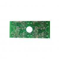
laser drilling Machining Broaching PCB Prototype Service Rapid Prototyping
PCB Prototype ServiceApplication - Multilayer Board
Multi-layer board: The required circuits are made on the front and
back surfaces of multiple double-sided boards, and an insulating
layer (Prepreg) is sandwiched between the two double-sided boards
and then pressed together to form several layers of copper. The
construction of the wire is usually an even number of layers due to
the use of multiple double-sided laminates. The number of copper
wires that can be made by multi-layer boards is the largest, and it
is used in more complex circuits. At present, the motherboards used
in computers mostly use eight-layer boards because of too many
components. Generally, small electronic products, such as mobile
phones, tablet computers, etc. Due to the requirement of small
size, at least an eight-layer board is required. The more
electronic components, the smaller the product size, and usually
more layers of PCB Prototype Service are required.
Material:
FR-4 (glass fiber epoxy resin substrate) is the most widely used
material in the global electronics industry. FR is a code name for
a flame-resistant material grade, which means a material
specification that the resin material must be able to
self-extinguish after burning. It is not a material name, but a
material grade, so there are many types of FR-4 grade materials
currently used in general circuit boards, but most of them are
four-functional epoxy resin plus filler (Filler) and glass fiber.
The composite material made. In recent years, due to the
development of electronic product installation technology and PCB
Prototype Service technology, FR-4 products with high Tg have
appeared again. Tg degree (glass transition temperature - Glass
Transition Temperature)
Example: ISOLA FR402, FR408, 370HR South Asia NP-140, NP-155, NP-175


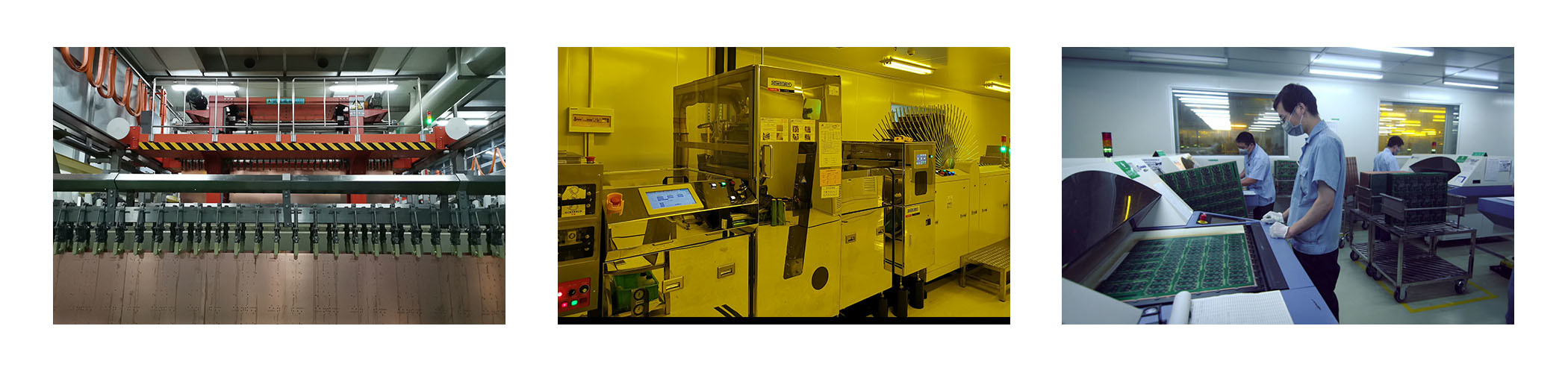
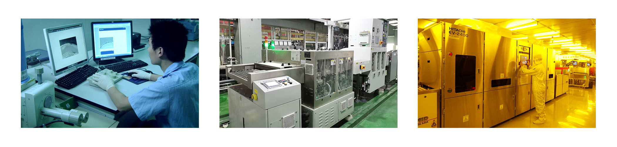
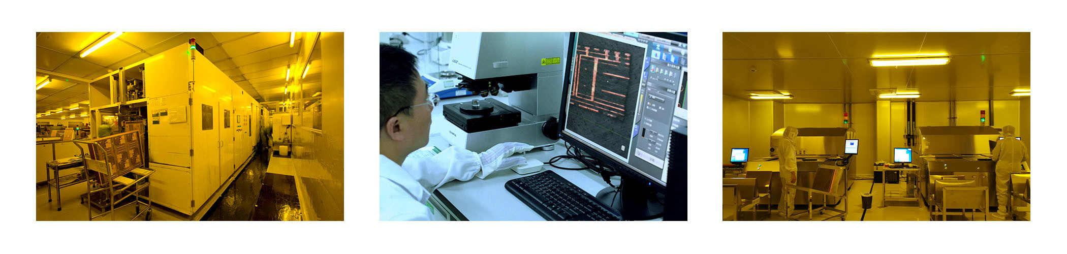
PCB Prototype service inspection method:
PCB Prototype service inspection methods include appearance optical
inspection and electrical path test
AOI (Auto Optical Inspection):
It is the automatic optical recognition system. Based on the
consideration of production efficiency and inspection accuracy, the
use of optical identification instruments to replace manual visual
inspection (Visual Inspection) is already a very basic process. The
principle of AOI is to first save the standard image file in the
device, use the image file to perform optical comparison with the
measured object, and automatically determine whether the error of
the measured object exceeds the standard. Scrap or repair. Since
the circuits on the circuit boards are getting more and more fine,
it has already exceeded the limit that can be found by the human
eye. Therefore, the AOI equipment of the PCB Prototype is mostly
used to check and compare the circuit layers, and compare whether
there is too much or too little etching or damage such as
collisions.
PCB Prototype Service Capacities and Technical Specification
Items | Capabilities | |
1 | Layers | 2-68L |
2 | Maximum machining size | 600mm*1200mm |
3 | Board thickness | 0.2mm-6.5mm |
4 | Copper thickness | 0.5oz-28oz |
5 | Min trace/space | 2.0mil/2.0mil |
6 | Minimum finished aperture | 0. 10mm |
7 | Maximum thickness to diameter ratio | 15:1 |
8 | Via treatment | Via, blind&buried via, via in pad, Copper in via … |
9 | Surface finish/treatment | HASL/HASL lead free, Chemical tin, Chemical Gold, Immersion gold Inmersion Silver/Gold, Osp, Gold Plating |
10 | Base Material | FR408 FR408HR, PCL-370HR;IT180A, Megtron 6(Panasonic);Rogers4350, |
11 | Solder mask color | Green.Black.Red.Yellow.White.Blue.Purple.Matte Green. Matte Black |
12 | Testing Service | AOI, X-Ray, Flying-Probe, Function Test, First Article Tester |
13 | Profiling Punching | Routing,V-CUT,Beveling |
14 | Bow&twist | ≤0.5% |
15 | HDI type | 1+n+1,2+n+2,3+n+3 |
16 | Min mechanical aperture | 0.1mm |
17 | Min laser aperture | 0.075mm |
Application advantages of multilayer circuit boards:
1. High assembly density, small size and light weight, meeting the
needs of lightweight and miniaturization of electronic equipment;
2. Due to the high assembly density, the wiring between components
(including components) is reduced, the installation is simple, and
the reliability is high;
3. Due to the repeatability and consistency of the graphics, wiring
and assembly errors are reduced, and equipment maintenance,
debugging and inspection time are saved;
4. The number of wiring layers can be increased, thereby increasing
design flexibility;
5. It can form a circuit with a certain impedance, and can form a
high-speed transmission circuit;
6. The circuit and magnetic circuit shielding layer can be set, and
the metal core heat dissipation layer can also be set to meet the
needs of special functions such as shielding and heat dissipation.


FAQ
Q: The lead-free process is required when the circuit board is
printed. What should I pay attention to when making the circuit
board? |
Q: Can your company provide the serial number when making circuit
board text? |
Q: How long is the shelf life of the PCB Prototype board and
how should it be stored? |
Q: What is your delivery date? |


