Active Member
|
[China]

Address: Building B, Shangxing West Industrial Zone, No. 1001, West Ring Road, Shajing street, Bao'an District, Shenzhen, Guangdong, China
Contact name:Yu

Quanhong FASTPCB |
|
|
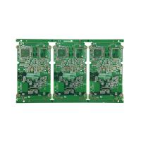
TG180 FR4 Fpga Quick Turn Rigid Flex Pcb 1.6mm FPGA Printed Circuit Board
FR-4 TG180 FPGA High Speed Printed Circuit Board
this board is 4 layer it is used for security equipment application. we can accept PCB prototype,samll volum, middle and large volume. no MOQ request for new order.all of our PCB are met UL, TS 16949,ROHS, ISO etc. certification.
| Item | HDI Advanced Technology | |||
| 2019 | 2020 | 2021 | ||
| Structure | 5+n+5 | 6+n+6 | 7+n+7 | |
| HDI Stack Via | AnyLayer(12L) | AnyLayer(14L) | AnyLayer(16L) | |
| Board Thickness(mm) | Min. 8L | 0.45 | 0.4 | 0.35 |
| Min. 10L | 0.55 | 0.45 | 0.4 | |
| Min. 12L | 0.65 | 0.6 | 0.55 | |
| MAX. | 2.4 | |||
| Min. Core Thickness ( um ) | 50 | 40 | 40 | |
| Min. PP Thickness ( um ) | 30(#1027PP) | 25(#1017PP) | 20(#1010PP) | |
| Base Copper Thickness | Inner Layer ( OZ) | 1/3 ~ 2 | 1/3 ~ 2 | 1/3 ~ 2 |
| Outer Layer ( OZ ) | 1/3 ~ 1 | 1/3 ~ 1 | 1/3 ~ 1 | |
| Item | HDI Advanced Technology | |||
| 2019 | 2020 | 2021 | ||
| Min. Mechanical Drill hole size(um) ** | 200 | 200 | 150 | |
| Max. Through Hole Aspect Ratio * | 8:1 | 10:1 | 10:1 | |
| Min. Laser via/Pad Size ( um ) | 75/200 | 70/170 | 60/150 | |
| Max. Laser Via Aspect Ratio | 0.8:1 | 0.8:1 | 0.8:1 | |
| Laser Via on PTH(VOP)design | Yes | Yes | Yes | |
| Laser X type through hole(DT≤200um) | NA | 60~100um | 60~100um | |
| Min. LW/S (L/S/Cu, um) | Inner Layer | 45 /45 /15 | 40/ 40/ 15 | 30/ 30 /15 |
| outer Layer | 50 /50/ 20 | 40 /50 /20 | 40 /40 /17 | |
| Min BGA Pitch (mm) | 0.35 | 0.3 | 0.3 | |
| Item | HDI Advanced Technology | |||
| 2019 | 2020 | 2021 | ||
| Solder mask Registration (um) | +/- 30 | +/- 25 | +/- 20 | |
| Min. Solder Mask Dam (mm) | 0.07 | 0.06 | 0.05 | |
| PCB Warpage Control | >= 50ohm | +/-10% | +/-8% | +/- 5% |
| < 50ohm | +/- 5ohm | +/- 3ohm | +/- 3ohm | |
| PCB Warpage Control | ≤0.5% | ≤0.5% | ≤0.5% | |
| cavity Depth accuracy (um) | Mechanical | +/- 75 | +/- 75 | +/- 50 |
| Laser directly | +/- 50 | +/- 50 | +/- 50 | |
| Surface Finishing | OSP,ENIG,Immersion Tin,Hard Au, Immersion Ag | OSP,ENIG,Immersion Tin,Hard Au,Immersion Ag, ENEPIG | ||
| Item | HLC Advanced Technology | |||
| 2019 | 2020 | 2021 | ||
| Max Panel Width (inch) | 25 | 25 | 25 | |
| Max Panel Length (inch) | 29 | 29 | 29 | |
| Max Layer Count (L) | 16 | 18 | 36 | |
| Max Board thickness (mm) | 3.2 | 4 | 6 | |
| Max Board thickness Tolerance | +/-10% | +/-10% | +/-10% | |
| Base copper Thickness | Inner layer ( OZ ) | 4 | 6 | 8 |
| Outer Layer ( OZ ) | 2 | 3 | 4 | |
| Min DHS ( mm ) | 0.2 | 0.15 | 0.15 | |
| PTH Size Tolerance ( mil ) | +/-2 | +/-2 | +/-2 | |
| Back Drill (stub)( mil ) | ~ 3 | ~ 2.4 | ~ 2 | |
| Max. AR | 12:1 | 16:1 | 20:1 | |
| Item | HLC Advanced Technology | |||
| 2019 | 2020 | 2021 | ||
| M-drill tolerance | Inner layer ( mil ) | DHS + 10 | DHS + 10 | DHS + 8 |
| Outer Layer ( mil ) | DHS + 8 | DHS + 8 | DHS + 6 | |
| Solder mask Registration (um) | +/- 40 | +/- 30 | +/- 25 | |
| Impedance control | ≥50ohms | +/-10% | +/-10% | -/-8% |
| <50ohms | 5 Ω | 5 Ω | 4 Ω | |
| Min LW/S (Inner)@1oz base Cu ( mil ) | 3.0 / 3.0 | 2.6 / 2.6 | 2.5 / 2.5 | |
| Min LW/S (Outer)@1oz Cu ( mil ) | 3.5 / 3.5 | 3.0 / 3.5 | 3.0 / 3.0 | |
| Max dimple for POFV ( um ) | 30 | 20 | 15 | |
| Surface Finishing | ENIG, Immersion Ag, OSP, HASL, Immersion Tin, Hard Au | |||
Packaging & Delivery | |||||
Packaging Details: | Inner: vacuum packing or Anti-static package, | ||||
Port: | Shenzhen or Hongkong | ||||
Lead Time: | Quantity(Pieces) | 1-10 | 11-100 | 101-1000 | >1000 |
| Est. Time(days) | 3-5 | 3-5 | 7-9 | To be negotiated |
Advantage Of PCB Printed Circuit Board
• Strict product liability, taking IPC-A-160 standard
• Engineering pretreatment before production
• Production process control (5Ms)
• 100% E-test, 100% visual inspection, including IQC, IPQC, FQC, OQC
• 100% AOI inspection, including X-ray, 3D microscope and ICT
• High-voltage test, impedance control test
• Micro section, soldering capacity, thermal stress test, shocking test
FAQ:
Q: What service do you have?
FASTPCB: We provide turnkey solution including PCB fabrication,
SMT, plastic injection & metal,final assembly, testing and
other value-added service.
Q: What is needed for PCB & PCBA quotation?
FASTPCB: For PCB: Quantity, Gerber file and technic
requirements(material,size, surface finish treatment, copper
thickness,board thickness).
For PCB: PCB information, BOM,Testing documents.
Q: How to keep our product information and design file secret ?
FASTPCB: We are willing to sign a NDA effect by customers side
local law and promising tokeep customers data in high confidential
level.
Q: What are the main products of your PCB/PCBA services?
FASTPCB: Automotive, Medical, Industry Control, IOT, Smart Home,
Military, Aerospace.
Q: What is your minimum order quantity (MOQ)?
FASTPCB: Our MOQ is 1 PCS, sample and mass production all can
support.
Q: Are you factory?
FASTPCB:Shangxing West Industrial Zone, Xihuan Road, Shajing
Street, Bao 'an District, Shenzhen, Guangdong province, China