

Active Member
|
[China]

Address: A1-405 (Exit A, Fuyong Metro Station), Fuhai Information Port, Bao'an District, Shenzhen. 10mins from Shenzhen Bao'an International Airport by subway
Contact name:Cyan Hong

Shenzhen Lefang Electronics Co., Ltd |
|
|
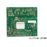
2 Layers FM Transmitter PCB Circuit Board for Communication Electronics
This double sided PCB board is used as mainboard in simple communication devices. The PCB board is 155.5 * 149.5 mm. And the min. aperture is 0.4 mm. Double sided PCB helps low the cost of PCB board but the size will be bigger than multilayer PCB.

Established in 1999, Lefang owns 3 modern Printed Circuit Board factories in Guangdong, China.
We provide One-stop solution for PCB & PCBA manufacturing to our customers home and abroad.
High quality PCB products, competitive price, on time delivery, after-sale service are always offered.
To make the continued progress, we try our best to in every section, including selecting quality raw materials
strictly, imported advanced automated equipments, employing 70 experienced engineers, acquiring global
certification of ISO9001:2008, ISO14001:2004, ISO/TS16949:2009, UL, QC080000, OHSA18000, etc.
Our customers' industry come from Communication, Industrial Control, Automotive, Medical Equipment,
Security Apparatus, Consumer Electronics and LED Lighting.
We sincerely pursue win-win business with customer all the time!
![]()
| Step 1 Please send us Gerber file with these format: .CAD / .Gerber / .PCB / .DXP / .P-CAD, etc | ||||||||||||||||||||
| Step 2 Also please provide us the below details for quick quotation: | ||||||||||||||||||||
Board material: Fr - 4 / CEM - 1 / CEM - 3 / 22F / Fr - 1 / others | ||||||||||||||||||||
| Material brand: SY / KB / Rogers (optional) | ||||||||||||||||||||
| Material Specification:High Tg / copper based / aluminum based or others (optional) | ||||||||||||||||||||
| Board thickness: 0.1 - 6.0 mm | ||||||||||||||||||||
| Copper thickness: 0.05 Oz - 8 Oz ( 17 um - 288 um ) | ||||||||||||||||||||
| Surface Treatment: OSP / ENIG / HASL / Lead Free HASL / Immersion Tin / Immersion Sin | ||||||||||||||||||||
| Color of solder mask and silk print: Green / red / blue / black / white / yellow ,etc | ||||||||||||||||||||
| Board size and quantity | ||||||||||||||||||||
If you don't have Gerber file, please provide us the imfomation as step 2 or post your PCB Board to us for clone.
| ||||||||||||||||||||
SAMPLE:
| ||||||||||||||||||||
| ||||||||||||||||||||
Lead Time
| Layer count | Sample lead time/workday | Batch lead time/workday |
| 1-2L | 2 | 6 |
| 4L | 5 | 8 |
| 6L | 5 | 9 |
| 8L | 6 | 10 |
| 10L | 8 | 10 |
| 12L | 8 | 12 |
| 14L | 10 | 15 |
| 16L | 10 | 18 |
| 18-40L (Up to difficulty) | at least 18 | at least 24 |
| P.S. For HDI, Blind/Buried Hole PCB: Regular Lead Time + 3 workdays | ||
What kinds of test function will be offered?
![]()
| AOI (Automated Optical Inspection) | Impedance control |
| Automatic short-circuit testing | Metallographic microscope |
| RoHS detector | Fly probe/ fixture mold |
| Dielectric tester | Visual inspection |
Now send us your inquiry, and you will be replied within 8 hours!
Little knowledge - High Tg PCB
The glass transition temperature (Tg) is an important normative dimension for the base material that determines the temperature at which the resin matrix converts from a glassy, brittle condition into a soft, elastic one.
Normally high Tg refers to high heat resistance in PCB raw material.
The standard Tg for copper clad laminate is between 130 – 140℃. High Tg is generally greater than 170℃, and middle Tg is generally greater than 150℃. Basically the printed circuit board with Tg≥170℃, we call high Tg PCB.
The higher of TG value, the better of pcb high temperature resistance.


