

Active Member
|
[China]

Address: A1-405 (Exit A, Fuyong Metro Station), Fuhai Information Port, Bao'an District, Shenzhen. 10mins from Shenzhen Bao'an International Airport by subway
Contact name:Cyan Hong

Shenzhen Lefang Electronics Co., Ltd |
|
|
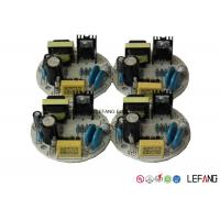
Advanced 100% Reliable PCB Board Assembly Contract EMS Electronics
This PCBa is order by a famous EMS company, the purchase pcb for their customers or they produce it.
This PCBa use white solder mask, OSP surface treatment and CEM-1 made PCB.
-- Lefang provides One-Stop solution to save your cost and time.
| Quick Quotation - Competitive factory price is always offered |
| Free Sample - Sample for free before mass production |
| Quality Control - Sales Team monitors the production quality and lead time |
| On Time Delivery - Customize the logistics plan according to customer’s requirement |
After-sale Service - Reply to the claim within 24 hours to make sure our customer’s manufacturing |
![]()
| Step 1 Please send us Gerber file with these format: .CAD / .Gerber / .PCB / .DXP / .P-CAD, etc | ||||||||||||||||||||
| Step 2 Also please provide us the below details for quick quotation: | ||||||||||||||||||||
Board material: Fr - 4 / CEM - 1 / CEM - 3 / 22F / Fr - 1 / others | ||||||||||||||||||||
| Material brand: SY / KB / Rogers (optional) | ||||||||||||||||||||
| Material Specification:High Tg / copper based / aluminum based or others (optional) | ||||||||||||||||||||
| Board thickness: 0.1 - 6.0 mm | ||||||||||||||||||||
| Copper thickness: 0.05 Oz - 8 Oz ( 17 um - 288 um ) | ||||||||||||||||||||
| Surface Treatment: OSP / ENIG / HASL / Lead Free HASL / Immersion Tin / Immersion Sin | ||||||||||||||||||||
| Color of solder mask and silk print: Green / red / blue / black / white / yellow ,etc | ||||||||||||||||||||
| Board size and quantity | ||||||||||||||||||||
If you don't have Gerber file, please provide us the imfomation as step 2 or post your PCB Board to us for clone.
| ||||||||||||||||||||
SAMPLE:
| ||||||||||||||||||||
| ||||||||||||||||||||
| Layer count | Sample lead time/workday | Batch lead time/workday |
| 1-2L | 2 | 6 |
| 4L | 5 | 8 |
| 6L | 5 | 9 |
| 8L | 6 | 10 |
| 10L | 8 | 10 |
| 12L | 8 | 12 |
| 14L | 10 | 15 |
| 16L | 10 | 18 |
| 18-40L (Up to difficulty) | at least 18 | at least 24 |
| P.S. For HDI, Blind/Buried Hole PCB: Regular Lead Time + 3 workdays | ||
-- What LEFANG's vision is to Make Our Customer's Products Better, so we try our best to fulfill the quality control
system andenvironmental management system. Our approved certification are as below:
| ISO9001:2008 | ISO14001:2004 |
| ISO/TS16949:2009 | OHSAS18000 |
| UL | RoHS |
| QC080000 | CQC |
Now send us your inquiry, and you will be replied within 8 hours!
Little knowledge - Multilayer PCB Board
Multilayer printed circuit boards (Multilayer PCBs) represented the next major evolution in fabrication technology.
A very sophisticated and complex methodology came from the base platform of double sided plated.
This methodology would again allow circuit board designers a dynamic range of interconnects and applications.
Multilayer PCB board were essential in the advancement of modern computing, and their basic construction and fabrication are similar to micro chip fabrication on a micro size.
The range of material combinations is extensive from basic epoxy glass to exotic ceramic fills, and it can be built on ceramic, copper, and aluminum. Also, blind and buried vias are commonly produced in multilayer pcb manufacturing, along with pad on via technology.


