

Active Member
|
[China]

Address: 4113-4116# A Area, HSST PARK, BAO'AN District, Shenzhen, China
Contact name:Wendy

Abis Circuits Co., Ltd. |
|
|
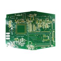
OEM FR4 Material Printed Circuit Board RoHS HDI Board Prototype PCB
Company Introduction:
Abis Circuits Co., Ltd is a professional PCB manufacturer which was established on Oct, 2006 and focus on double side, Multilayer and HDI PCB mass production. We have two factories together , the factory in Shenzhen is specialized in small and middle volume orders and the factory in Jiangxi province is for big volume and HDI. Our aim is help the clients gain more competitive strength and bring more mutual benefit to each other. All clients will be served well.
What is a HDI PCB?
IPC-2226 defines HDI as a printed circuit board with a higher wiring density per unit area than conventional printed circuit boards (PCB). They have finer lines and spaces ≤ 100 µm / 0.10mm, smaller vias (<150 µm) and capture pads <400 µm / 0.40mm, and higher connection pad density (>20 pads/cm2) than employed in conventional PCB technology.
Product We Produce:
1. Rigid, Flex, Rigid-Flexible PCB.
2. Buried/Blind Vias, Via in Pad, Counter Sink Hole, Screw
Hole(Counterbore), Press-fit, Half Hole.
3. HASL lead-free, Immersion Gold/ Silver/Tin, OSP, Gold
plating/finger, Peelable mask,
4. Printed Circuit Boards adhere to IPC Class 2 & 3
international PCB standard.
5. Quantities range from prototype to medium & big batch
production.
6. 100% E-test
Product Description
| Item | Production Capacity |
| Layer Counts | 1-20 layers |
| Material | FR-4,Cu base,High TG FR-4,PTFE,Rogers,TEFLON etc. |
| Board thickness | 0.20mm-8.00mm |
| Maximum Size | 600mmX1200mm |
| Board Outline Tolerance | +0.10mm |
| Thickness Tolerance(t≥0.8mm) | ±8% |
| Thickness Tolerance(t<0.8mm) | ±10% |
| Insulation Layer Thickness | 0.075mm--5.00mm |
| Minimum Line | 0.075mm |
| Minimum Space | 0.075mm |
| Out Layer Copper Thickness | 18um--350um |
| Inner Layer Copper Thickness | 17um--175um |
| Drilling Hole(Mechanical) | 0.15mm--6.35mm |
| Finish Hole(Mechanical) | 0.10mm-6.30mm |
| Diameter Tolerance(Mechanical) | 0.05mm |
| Registration(Mechanical) | 0.075mm |
| Aspect Ratio | 16:1 |
| Solder Mask Type | LPI |
| SMT Mini.Solder Mask Width | 0.075mm |
| Mini. Solder Mask Clearance | 0.05mm |
| Plug Hole Diameter | 0.25mm--0.60mm |
| Impedance control Tolerance | ±10% |
| Surface finish/treatment | HASL,ENIG,Chem,Tin,Flash Gold, OSP, Gold Finger |
Capacity
| Max. No. of Layers | 20 |
| Max. Board Size | 860*610mm |
| Board Thickness | 0.2-6.0mm |
| Copper Thickness | 0.5OZ-6OZ |
| Material | Various |
| Surface Finish | Various |
| Soldermask | Various |
| Minimum Soldermask Thickness | 0.025mm |
| Minimun Soldermask BridgeDam | 0.15mm |
| Minimum Soldermask Clearance | 0.075mm |
| Peelable Colours | Blue |
| Peelable Minimum Feature | 0.5mm |
| Peelable Maximum Tented Hole | 3.0mm |
| Scoring Angle | 30 Degrees |
| Min. Remaining Thickness | 0.3mm |
| Min. Distance to copper (From center of scoring line) | 0.5mm |
| Min. Track | 0.1mm |
| Min.Gap(TrackTrack,TrackPad,PadPad) | 0.1mm |
| NPTH Min. Drill Size | 0.2mm |
| Plated Drill Size | ± 0.075mm |
| Non-Plated Drill Size | ± 0.05mm |
| Drill Location Tolerance | ± 0.05mm |
| OutlineRouted Slots | ± 0.1mm |
| Line Width/Spacing | ±10% |
| Board Thickness | ±10% |
| Warp and Twist | 0.05% |
| Scoring/V-Cut | ± 5 degrees |
| Scoring Positional Tolerance | ± 0.1mm |
| Aspect Ratio | 10:01 |
Lead Time
| Number of Layers | Quick Turn Lead Time |
| 2 | 24 Hours |
| 4 | 48 Hours |
| 6 | 72 Hours |
| 8 | 96 Hours |
| 10 | 120 Hours |
| 12 | 120 Hours |
| 14 | 144 Hours |
| 16 | Depend on Technical Specification |
| 18 | Depend on Technical Specification |
| 20 | Depend on Technical Specification |
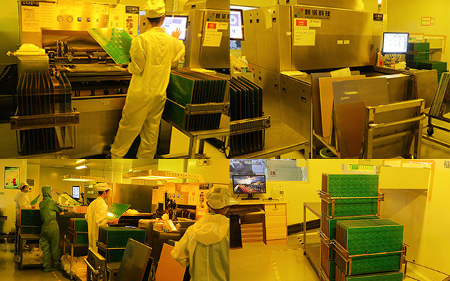
Work Shop

Certificate

Q1:Are you a factory or trade company?
A: Abis is a PCB/FPC/PCBA manufacturer/factory. We pecialize in PCB/PCBA Board for 12 years.
Q2:Is my PCB file safe if I send it to you for manufacturing?
A: We respect customer's design authority and will never
manufacture PCB for someone else without your permission. NDA is
acceptable.
Q3:What is your testing policy and how you control the quality?
A: For sample, usually tested by flying probe; for PCB Volume over
3 square meters, usually tested by fixture, this will be more
faster. Due to there's many steps to PCB production, we usually do
inspection after every step.
Q4: What's your shipping way ?
A: 1. We have our own forwarder to ship goods by DHL, UPS, FEDEX,
TNT,EMS.
2. If you have your own forwarder, we can cooperate with them.
Q5: What is your certificate?
A: ISO9001:2015, ISO14001: 2015, UL, SGS,RoHS report.
Q6: What files should we offer?
A: If only need PCB, please provide Gerber File and manufacturing
specifications; If need PCBA,Please provide Gerber File,
Manufacturing specification, BOM list and Pick & Place/XY file.
Q7: Can I get a sample?
A: Yes, It's reasonable to get a sample to test our quality at
first.
Q8:How about the payment terms?
A:By T/T, Paypal, Western Union, etc.
ABIS cares every your order even 1 piece


