

Active Member
|
[China]

Address: 4113-4116# A Area, HSST PARK, BAO'AN District, Shenzhen, China
Contact name:Wendy

Abis Circuits Co., Ltd. |
|
|
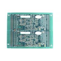
High Density Automotive Iteq180 Printed Circuit Board With Immersion Goldwith Buried Bline Vias
Introduction
Abis Circuits Co., Ltd is a professional PCB manufacturer which was established on Oct, 2006 and focus on double side, Multilayer and HDI pcb mass production.
ABIS Histories
2006 ABIS Electronics Founded, and Set up the factory in Shenzhen
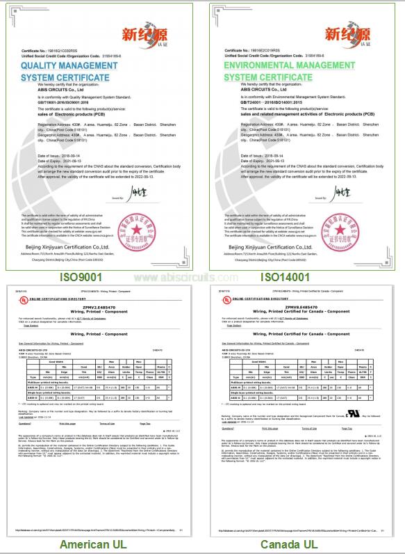
2008 Shenzhen Factory Put into Production and Passed the certification
of America UL and ISO9001
2009 Shenzhen Factory got Canada UL.and Start to make 16 Layers in
Volume
2010 Overseas Sales Department ABIS Circuits Co., Ltd established
2010 Acquired the ISO14001 environmental management system
certification
2012 The manufacturing equipment was updated and a batch of
cutting-edge manufacturing equipment was imported from Sweden,
France, the United States, Germany, and other countries
2015 We have an investment in our Subcontractor in Jiangxi, No of
Employees 1200 with 5000 square meters, the plant monthly product
capability reached to 40,000m2
2016 The team was refined, and all staff participated in the
development training to create a wolf team
2017 Attend Expo Electronica 2017/ electronica India
2018 Attend Expo Electronica 2018/Electronica India
2019 Attend Expo Electronica 2019/ Electronica India
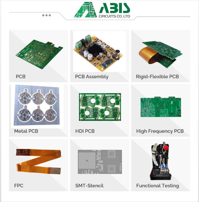
Product Details
1. Rigid, Flex, Rigid-Flexible PCB.
2. Buried/Blind Vias, Via in Pad, Counter Sink Hole, Screw Hole(Counterbore), Press-fit, Half Hole.
3. HASL lead-free, Immersion Gold/ Silver/Tin, OSP, Gold plating/finger, Peelable mask,
4. Printed Circuit Boards adhere to IPC Class 2 & 3 international PCB standard.
5. Quantities range from prototype to medium & big batch production.
Lead Time
| Category | Q/T Lead time | Standard Lead Time | Mass Production | |||
| 2 Layers | 24hrs | 3-4 working days | 8-15 working days | |||
| 4 Layers | 48hrs | 3-5 working days | 10-15 working days | |||
| 6 Layers | 72hrs | 3-6 working days | 10-15 working days | |||
| 8 Layers | 96hrs | 3-7 working days | 14-18 working days | |||
| 10 Layers | 120hrs | 3-8 working days | 14-18 working days | |||
| 12 Layers | 120hrs | 3-9 working days | 20-26 working days | |||
| 14 Layers | 144hrs | 3-10 working days | 20-26 working days | |||
Capacity
| Item | Spec |
| Layers | 1~20 |
| Board Thickness | 0.1mm-8.0mm |
| Material | FR-4, CEM-1/CEM-3, PI, High Tg, Rogers, PTEF, Alu/Cu Base, etc |
| Max Panel Size | 600mm×1200mm |
| Min Hole Size | 0.1mm |
| Min Line Width/Space | 3mil(0.075mm) |
| Board Outline Tolerance | 士0.10mm |
| Insulation Layer Thickness | 0.075mm--5.00mm |
| Out Layer Copper Thickness | 18um--350um |
| Drilling Hole (Mechanical) | 17um--175um |
| Finish Hole (Mechanical) | 0.10mm--6.30mm |
| Diameter Tolerance (Mechanical) | 0.05mm |
| Registration (Mechanical) | 0.075mm |
| Aspect Ratio | 16:01 |
| Solder Mask Type | LPI |
| SMT Mini. Solder Mask Width | 0.075mm |
| Mini. Solder Mask Clearance | 0.05mm |
| Plug Hole Diameter | 0.25mm--0.60mm |
| Impedance Control Tolerance | 士10% |
| Surface finish | ENIG, OSP, HASL, Chem. Tin/Sn, Flash Gold |
| Soldermask | Green/Yellow/Black/White/Red/Blue |
| Silkscreen | Red/Yellow/Black/White |
| Certificate | UL, ISO 9001, ISO14001, IATF16949 |
| Special Request | Blind hole, Gold finger, BGA, Carbon ink, peelable mask, VIP process, Edge plating, Half holes |
| Material Suppliers | Shengyi, ITEQ, Taiyo, etc. |
| Common Package | Vacuum+Carton |
Related product
Certificate
FAQ
Q1:When can I get the quotation?
A:We usually quote with 1 hour after we get your inquiry. If you are
very urgent, please call us or tell us in your email.
Q2:Can you provide free samples for me?
A:Free samples depend on your order quantity.
Q3:I am a small wholesaler, do you accept small order?
A:It's no problem. If you're small wholesaler, we would like to grow
up with you together.
Q4:How many days will samples be finished? And how about the mass
production?
A:Generally 2-3 days for samples making. The lead time of mass
production will depend on the order quantity and the season you
place the order.
Q5:If I order big quantity, what's the good price?
A:Please send the details enquiry to us, such as the Item Number,
Quantity for each item, Quality request, Logo, Payment Terms,
Transport method, Discharge place etc. We will make the accurate
quotation to you as soon as possible.
Q6: How can we know the processing about PCB order?
A: Each Customer will have a sale to contact with you. Our
working hours: AM 9:00-PM 19:00(Beijing Time) from Monday to
Friday. We will reply your email as soon as quickly during our
working time. And you also could contact with our sales by
cellphone if urgent.
Q7:What is the shipping method?
A:We suggest you using DHL, UPS, FedEX, TNT forwarder.
Q8:How about the payment terms?
A:By T/T, Paypal, Western Union, etc.
(ABIS cares every your order even 1 piece)


