Active Member
|
[China]

Address: 4113-4116# A Area, HSST PARK, BAO'AN District, Shenzhen, China
Contact name:Wendy

Abis Circuits Co., Ltd. |
|
|
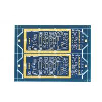
1. 12 layer PCB.
2. FR4 High Tg substrate.
3. Blind via,Buried via,VIP process.
4. Telecommunication application.
5. 0.063mm line width/space.
| 1 | Layers | 12 layer |
| 2 | Material | FR4 high tg |
| 3 | PCB thick | 1.65mm |
| 4 | Usage | Telecommunication |
| 5 | Microvia | 0.1mm |
| 6 | Min line track | 0.063mm |
| 7 | Min space | 0.063mm |
| 8 | Surface finish | ENIG 3u'' |
| 9 | Copper weight | 1OZ inner and 2OZ outer |
| 10 | Soldermask | Blue |
| 11 | Blind via | Yes |
| 12 | Buried via | Yes |
| 13 | Pads over via | Yes |
| 14 | blind via resin hole + plating filled | Yes |
| 15 | Certificates | UL,RoHS,ISO9001/14001,SGS,ISO/TS16949 |
FAQ
Q1:What's HDI?
A: High density Interconnect.
Q2:HDI description?
A: PCB with a higher wiring density per unit area than
conventional PCB,They have finer line and space<=0.1mm,smaller
via(<=0.15mm) and capture pad<=0.4mm, and higher connection
paddensity(>20pads/cm2) than conventional one.
Q3:Quality policy?
A: All HDI board test fine then shipment.
Q4: How about delivery?
A: 20 working days production time for HDI PCB.
Q5: Application area?
A: Telecommunication,Control system,Electronics,Lighting and so on.
Q6: What's the important file requirement?
A: Gerber file besides drill chart/layer.
Factory visitor: