
|
|
[China]

Trade Verify
Address: Building C5/B6, Yanchuan North Industrial Park, Yanluo Street, Baoan District, Shenzhen, China
Contact name:Rachel

Shenzhen Benqiang Circuits Co,Ltd. |
|
Verified Suppliers
|
|
|
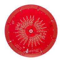
High Layer PCB with Min. Hole Size 0.2mm and HASL Surface Finish for High Layer Designs
High Layer PCB is a top grade printed board designed to meet the demanding needs of advanced electronic devices. This high-quality product is made with FR-4 material, ensuring durability and reliability for your electronic projects.
Our High Layer PCB boasts a high-layer design that allows for multiple layers of circuitry, making it suitable for complex and high-speed electronic applications. This advanced design also ensures better signal integrity and reduces interference, resulting in superior performance.
With the use of impedance control technology, our High Layer PCB offers precise control over the electrical characteristics of the circuit. This allows for consistent and accurate signal transmission, ensuring high-quality and reliable operation of your electronic devices.
Our High Layer PCB is designed with a minimum hole size of 0.2mm, allowing for microscopic designs to be implemented with precision. This enables the creation of compact and high-density electronic devices without compromising on performance.
In addition to the high precision and intricate design, our High Layer PCB also offers a minimum solder mask clearance of 0.1mm. This provides optimal protection against solder bridging and ensures the reliability and longevity of your electronic devices.
Our High Layer PCB is manufactured using advanced production techniques and state-of-the-art equipment. This ensures the highest level of quality control and guarantees that every product meets our strict standards of excellence.
When it comes to high-grade PCBs, our High Layer PCB is the top choice for professionals in the electronics industry. With its advanced design, quality materials, and precision control, it is the perfect solution for your high-performance electronic projects. Order now and experience the difference in quality and performance with our High Layer PCB.
| Product Name | High Layer PCB |
|---|---|
| Surface Finish | HASL, ENIG, OSP, Immersion Silver, Immersion Tin |
| Material | FR-4 |
| Layer Count | High Layer |
| Solder Mask Color | Green, Blue, Black, Red, Yellow, White |
| Min. Line Width/Spacing | 3mil/3mil |
| Min. Solder Mask Clearance | 0.1mm |
| Lead Time | 3-5 Days |
| Copper Thickness | 1/3 Oz To 2 Oz |
| Board Thickness | 0.2mm To 6.0mm |
| Rohs Compliant | Yes |
The High layer PCB, also known as the Superior printed wiring board, is a type of printed circuit board that is designed for precision electronics and high-speed signal transmission. It has become an essential component in the electronics industry, as it provides a reliable and efficient platform for various electronic devices.
With its advanced features and capabilities, the High layer PCB is widely used in a variety of applications and scenarios. Let's take a closer look at some of its most common applications and scenes:
The High layer PCB is often used as the top layer printed board in high-end electronic devices such as smartphones, laptops, and gaming consoles. Its superior design and construction make it the perfect choice for these advanced devices. The High layer PCB's ability to handle high-speed signal transmission and its precise wiring ensure the smooth functioning of these devices.
In the industrial sector, the High layer PCB is widely used as the upper-tier printed circuitry in equipment and machinery. Its high-quality construction and reliable performance make it the ideal choice for industrial applications. The High layer PCB can withstand extreme temperatures, vibrations, and other harsh conditions, making it suitable for use in various industrial settings.
Another important application of the High layer PCB is in the medical industry. Its precise wiring and high-speed signal transmission capabilities make it the perfect choice for medical devices such as ultrasound machines, patient monitors, and MRI scanners. The High layer PCB's ability to handle complex and sensitive data makes it an essential component in precision medical equipment.
The High layer PCB is also widely used in high-speed communication networks such as 5G and fiber optic networks. Its ability to handle high-speed signal transmission and its low signal loss make it the preferred choice for these networks. The High layer PCB's design also allows for faster data transfer, making it crucial for the smooth functioning of these networks.
In the aerospace and defense industry, the High layer PCB plays a critical role in the functioning of various electronic systems and equipment. Its high performance and reliability make it the ideal choice for use in aircraft, satellites, and military equipment. The High layer PCB's ability to withstand extreme conditions and its precise wiring make it essential for these applications.
In conclusion, the High layer PCB's solder mask colors, including green, blue, black, red, yellow, and white, along with its minimum hole size of 0.2mm, board thickness of 0.2mm to 6.0mm, and minimum silkscreen clearance and solder mask clearance of 0.15mm and 0.1mm respectively, make it a versatile and highly sought-after product in the electronics industry. Its applications and scenes range from high-end consumer electronics to critical industrial and medical equipment, proving its importance and impact in the world of precision electronics and high-speed signal transmission.
At High Layer PCB, we offer top-of-the-line customization services for high-grade printed circuit boards. Our team of experts is dedicated to providing you with the best quality and performance for your specific needs.
With our high-level printed circuit boards, we offer a wide range of customization options to meet your specific requirements.
Some of our customization services include:
Our team of experienced engineers will work closely with you to understand your unique needs and provide you with the best solutions for your high-grade PCB.
Choosing High Layer PCB for your customization needs means choosing quality, reliability, and performance. Some of the key reasons to choose us include:
Trust us to provide you with the best customization services for your high-grade PCB needs. Contact us today to discuss your requirements and get a quote for our services.
After manufacturing and testing, the High Layer PCB will be carefully packaged to ensure its safe delivery to the customer. The packaging process includes the following steps:
Once packaged, the High Layer PCB will be shipped to the customer using a reliable shipping method. The shipping process includes the following steps:
With our careful packaging and reliable shipping methods, we guarantee that the High Layer PCB will arrive at its destination in perfect condition.


