

Active Member
|
[China]

Address: Building C5/B6, Yanchuan North Industrial Park, Yanluo Street, Baoan District, Shenzhen, China
Contact name:sales

Shenzhen Benqiang Circuits Co,Ltd. |
|
|
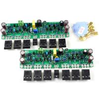
FR-4 Communication Printed Circuit Board Assembly for with ENIG Surface Finish
Communication PCB Assembly is a specialized product designed for communication systems and devices. It is a crucial component in ensuring smooth and efficient communication between different devices and systems.
The PCB (Printed Circuit Board) used in Communication PCB Assembly is processed with Immersion Gold, a type of surface finish that provides excellent conductivity, solderability, and durability. It is an ideal choice for communication systems as it ensures stable and reliable performance.
Each Communication PCB Assembly undergoes a 100% E-Test, a type of electronic testing method that checks for any potential defects in the PCB. This ensures the quality and reliability of the product, minimizing the risk of failure in the communication system.
The PCB material used in Communication PCB Assembly is FR-4, a type of flame-retardant fiberglass material that is widely used in the electronics industry. It offers high strength, good insulation, and excellent thermal resistance, making it an ideal choice for communication systems.
Communication PCB Assembly requires Gerber and BOM (Bill of Materials) files for the PCB fabrication process. Gerber files contain the design information of the PCB, while BOM lists all the components and materials needed for the assembly. These files are crucial in ensuring accurate and efficient production of the PCB.
The project for Communication PCB Assembly involves the processing of incoming materials to ensure the quality and compatibility of all components used in the assembly. This includes thorough inspection and testing of all materials before they are used in the production process.
In conclusion, Communication PCB Assembly is a high-quality and reliable product that plays a crucial role in communication systems and devices. With its use of Immersion Gold process, 100% E-Test, FR-4 material, and strict processing of incoming materials, it offers excellent performance, stability, and durability for seamless communication.
| Communication PCB Assembly | |
|---|---|
| Pcb Material | FR-4 |
| Feature | High Reliability And Precision |
| Material | FR-4 |
| Project | Processing Of Incoming Materials |
| Test | 100% E-Test |
| Pcb Layers | 6 Layers |
| Material Of Pcb | FR-4 |
| Base Material | Copper |
| Min Hole Diameter | 0.1mm |
| Item | PCB Assembly |
| Communication Device PCB Assembly | |
|---|---|
| Pcb Material | FR-4 |
| Feature | High Reliability And Precision |
| Material | FR-4 |
| Project | Processing Of Incoming Materials |
| Test | 100% E-Test |
| Pcb Layers | 6 Layers |
| Material Of Pcb | FR-4 |
| Base Material | Copper |
| Min Hole Diameter | 0.1mm |
| Item | PCB Assembly for Communication Equipment |
The Communication PCB Assembly is a specialized circuit board designed specifically for communication equipment. It plays a crucial role in ensuring smooth and efficient communication between devices. With its high-quality materials and advanced surface finishes, this product is the perfect choice for any communication network assembly board.
The material used in the production of the Communication PCB Assembly is FR-4, a fire-retardant and high-performance material that is commonly used in the electronics industry. This material is known for its excellent electrical insulation properties, making it ideal for communication circuits.
Furthermore, the Communication PCB Assembly offers a variety of surface finishes to choose from, including HASL, ENIG, OSP, and Immersion Silver. Each surface finish has its unique advantages, making this product versatile and suitable for various applications.
The Communication PCB Assembly is primarily used in communication equipment such as routers, modems, and switches. These devices require a reliable and stable connection to ensure seamless communication between devices. The high-quality materials and surface finishes of this product provide excellent electrical conductivity, making it the perfect choice for this application.
Moreover, the Communication PCB Assembly is also widely used in AI Android Smart Modules. These modules require a high-performing circuit board to enable them to process complex algorithms and perform various tasks efficiently. The Communication PCB Assembly's FR-4 material and advanced surface finishes make it an ideal choice for these modules.
The Communication PCB Assembly can be easily customized to meet specific requirements with its Gerber&BOM Pcb request. This allows for precise and accurate production of the circuit board, ensuring a perfect fit for any communication equipment or AI Android Smart Module.
The Communication PCB Assembly is a vital component in the world of communication technology. Its high-quality materials, advanced surface finishes, and customizable options make it the perfect choice for any communication circuit board assembly. With this product, you can ensure reliable connections and smooth communication between devices, making it a must-have for any communication equipment or AI Android Smart Module.
This service is designed for the production of Communication PCB Assembly, specifically for Communication Devices. Our team of experts will work with you to create high-quality and reliable Communication Circuit Board Assembly that meets your exact specifications.
Our base material for the PCB is copper, known for its excellent conductivity and strength. The PCB material we use is FR-4, a widely-used and reliable material in the industry. We also provide customized Gerber and BOM files for your specific PCB requests.
Our specialized service is perfect for the production of 4G Communication/Network Switches. We understand the importance of high-speed and efficient communication in today's world, and our PCBAs are designed to meet those needs. The material of our PCB is FR-4, which provides excellent insulation and durability for your communication devices.
Choose our Electronics Assembly for Communication Devices and experience the benefits of our high-quality and reliable services. Our team is dedicated to providing you with top-notch PCBAs that meet your unique requirements. Contact us now to learn more about our customized services for Communication PCB Assembly.
Our Communication PCB Assembly products are carefully packaged and shipped to ensure safe and timely delivery to our customers. We take great care in the packaging process to protect the delicate components and prevent any damage during transportation.
Each PCB assembly is first placed in an anti-static bag to protect it from any static electricity. The bag is then placed in a sturdy cardboard box with sufficient cushioning material to prevent any movement or impact. We also use bubble wrap or foam padding to provide extra protection for more fragile components.
For international shipments, we comply with all necessary customs and export regulations. We label our packages with all the required shipping and handling information, including product name, quantity, weight, and destination address. We also provide all the necessary documentation, such as commercial invoices, packing lists, and certificates of origin.
We work with trusted and reliable shipping partners to ensure timely and cost-effective delivery. Our products can be shipped via air, sea, or land, depending on the customer's preference and urgency. We also offer expedited shipping options for urgent orders.
Customers can track their order and receive updates on the shipping status through our online tracking system. We strive to provide transparent and efficient communication throughout the shipping process to ensure customer satisfaction.
At Communication PCB Assembly, we understand the importance of timely and safe delivery, and we take all necessary measures to ensure our products reach our customers in perfect condition. Contact us for more information on our packaging and shipping process.


