

Active Member
|
[China]

Address: CSCES strait screen and core intelligent manufacturing base,Shuangliu District,Chengdu City, Sichuan Province, P. R. China
Contact name:Tyra

ZEIT Group |
|
|
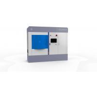
Magnetron Sputtering Deposition in Optical recording Industry
Applications
| Applications | Specific Purpose | Material Type |
| Optical recording | Phase change disc recording film | TeSe, SbSe, TeGeSb, etc |
| Magnetic disk recording film | TbFeCo, DyFeCo, TbGdFeCo, TbDyFeCo | |
| Optical disc reflective film | AI, AITi, AlCr, Au, Au alloy | |
| Optical disc protection film | Si3N4, SiO2+ZnS |
Working Principle
The working principle of magnetron sputtering is that electrons collide with argon atoms in the process of flying to
the substrate under the action of electric field, and make them ionized Ar cations and new electrons.while the new
electrons flying to the substrate, Ar ions fly to the cathode target at a high speed under the action of electric field
and bombard the target surface with high energy to make the target sputtered. Among the sputtered particles,
neutral target atoms or molecules are deposited on the substrate to form films, however, the generated secondary
electrons drift to the direction indicated by E (electric field) ×B (magnetic field) under the action of electric and
magnetic fields (“E×B shift”), their motion paths are similar to a cycloid. If under a toroidal magnetic field, the
electrons will move in a circle approximate to cycloid on the target surface. Not only the electron' motion paths are
fairly long, but also they are bounded in the plasma region near the target surface, where plenty of Ar are ionized
to bombard the target, thus realizing the high deposition rate. As the number of collisions increases, secondary
electrons use up their energy, gradually move away from the target surface and finally deposit on the substrate
under the action of electric field. Due to low energy of such electron, the energy transferred to the substrate is very
small, resulting in lower temperature rise of the substrate.
Features
| Model | MSC-OR-X—X |
| Coating type | Various dielectric films such as metal film, metal oxide and AIN |
| Coating temperature range | Normal temperature to 500℃ |
| Coating vacuum chamber size | 700mm*750mm*700mm (Customizable) |
| Background vacuum | < 5×10⁻⁷mbar |
| Coating thickness | ≥ 10nm |
| Thickness control precision | ≤ ±3% |
| Maximum coating size | ≥ 100mm (Customizable) |
| Film thickness uniformity | ≤ ±0.5% |
| Substrate carrier | With planetary rotation mechanism |
| Target material | 4×4 inches(compatible with 4 inches and below) |
| Power supply | The power supplies such as DC, pulse, RF, IF and bias are optional |
| Process gas | Ar, N2, O2 |
| Note: Customized production available. | |
Coating Sample

Process Steps
→ Place the substrate for coating into the vacuum chamber;
→ Roughly vacuumize;
→ Turn on molecular pump, vacuumize at top speed, then turn on the revolution and rotation;
→ Heating the vacuum chamber until the temperature reaches the target;
→ Implement the constant temperature control;
→ Clean elements;
→ Revolve and back to the origin;
→ Coating film according to process requirements;
→ Lower temperature and stop the pump assembly after coating;
→ Stop working when the automatic operation is finished.
Our Advantages
We are manufacturer.
Mature process.
Reply within 24 working hours.
Our ISO Certification

Parts Of Our Patents


Parts Of Our Awards and Qualifications of R&D


