
|
|
[China]

Trade Verify
Address: Building 1, Huafeng Science and Technology Park, No. 54 Guangtian Road, Luotian County community, Songgang Town, Bao'an District, Shenzhen City
Contact name:Sales Manager

ShenZhen Jieteng Circuit Co., Ltd. |
|
Verified Suppliers
|
|
|
The Silkscreen Color options available for our Multi-Level Printed Wiring Board Creation include White, Black, Yellow, and other colors as per the customer's request. This ensures that the PCBs are easy to read and identify, as well as aesthetically pleasing.
Our Surface Finish options for Multi-Level Printed Wiring Board Creation include HASL, ENIG, OSP, Immersion Silver, Immersion Tin, and other finishes as per the customer's request. This ensures that the PCBs are protected from oxidation, corrosion, and other environmental factors that can affect their performance and lifespan.
The Min. Hole Size for our Multi-Level Printed Wiring Board Creation is 0.2mm, ensuring that the PCBs are small and compact. This makes them ideal for use in high-density applications where space is at a premium.
Our Copper Thickness options for Multi-Level Printed Wiring Board Creation include 1-4oz, ensuring that the PCBs have the right amount of conductivity for their intended application. This ensures that the PCBs are able to carry the necessary signals and power without any issues.
The Min. Line Width for our Multi-Level Printed Wiring Board Creation is 0.1mm, ensuring that the PCBs have the necessary level of precision and accuracy. This is important for applications where the PCBs need to be able to carry high-speed signals or other sensitive data.
Our Multilayer PCB Fabrication service provides:
The Multilayer PCB Fabrication product is ideal for various application occasions and scenarios such as:
The Multilayer PCB Fabrication product is also suitable for other application scenarios such as aerospace, telecommunications, and military applications. With a minimum hole size of 0.2mm, this product offers high flexibility and versatility, making it an ideal choice for various PCB creation requirements.
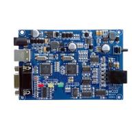
Our brand, JIETENG, offers high-quality Multi-Layer Printed Circuit Board production services. Our Model Number for this product is PCB circuit board, which is manufactured in our factory in China. We offer customization services to meet specific requirements of our clients.
The Board Thickness of our Multi-Layer Printed Circuit Board Production ranges from 0.2mm to 3.2mm, with Impedance Control for stable signal transmission. Our Min. Line Width is 0.1mm, and the Min. Hole Size is 0.2mm to ensure precision and accuracy.
We offer a variety of Solder Mask Colors including Green, Blue, White, Black, Red, and more. With our Multi-Level Printed Circuit Board Fabrication process, we can provide customized solutions for all your PCB needs.
Our Multilayer PCB Fabrication product technical support team is available to assist with any questions or issues you may have with the product. We offer troubleshooting assistance, product recommendations, and guidance on best practices for use.
In addition to technical support, we also provide a range of services to help ensure the success of your project. Our services include PCB layout and design, prototype fabrication, and full-scale production runs.
Our team is dedicated to providing the highest level of support and service to our customers. Contact us today to learn more about our Multilayer PCB Fabrication product and how we can assist with your project needs.
Product Packaging:
The Multilayer PCB Fabrication product will be packed securely in anti-static bags and then placed in a sturdy cardboard box with ample padding to protect it during transit. The box will be labeled with the product name and specifications for easy identification.
Shipping:
The Multilayer PCB Fabrication product will be shipped via a reputable courier service such as FedEx or DHL. The shipping cost will be calculated based on the weight and destination of the package. The customer will be provided with a tracking number to monitor the status of their shipment.


