
|
|
[China]

Trade Verify
Address: Building 1, Huafeng Science and Technology Park, No. 54 Guangtian Road, Luotian County community, Songgang Town, Bao'an District, Shenzhen City
Contact name:Sales Manager

ShenZhen Jieteng Circuit Co., Ltd. |
|
Verified Suppliers
|
|
|
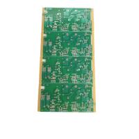
Multilayer PCB Fabrication is a leading manufacturer of high-quality multi-layer printed circuit boards (PCBs). We specialize in the creation of multi-level printed wiring boards that are used in a wide range of electronic devices, from smartphones and laptops to medical equipment and aerospace technology.
Our multi-layer PCBs are made with copper thickness ranging from 1-4oz, providing excellent conductivity and ensuring efficient performance of your electronic devices. We use state-of-the-art technology and advanced techniques to ensure precise copper thickness and smooth surface finish for optimal functionality.
With our advanced manufacturing processes, we are able to achieve a minimum line spacing of 0.1mm, allowing for more complex and compact circuit designs. This ensures that our multi-layer PCBs are able to meet the demands of modern electronic devices that require high-density circuits in a small form factor.
Our multi-layer PCBs are available in a range of board thicknesses from 0.2mm to 3.2mm, allowing for versatility in your PCB design. Whether you need a thin and lightweight board for portable devices or a thicker board for more robust applications, we have the capability to deliver the perfect solution for your specific needs.
To ensure the accuracy and precision of our multi-layer PCBs, we are able to achieve a minimum line width of 0.1mm. This enables us to create intricate and complex circuit patterns, making our PCBs suitable for a wide range of applications that require high-performance and reliability.
We offer a variety of material options to meet the specific requirements of your multi-layer PCB. Our options include FR4, High TG FR4, Halogen Free, Rogers, and more. Each material has its own unique properties, allowing us to cater to a wide range of applications and industries.
With years of experience in the industry, we have the expertise and capabilities to deliver high-quality multi-layer PCBs that meet the strictest quality standards. Our manufacturing processes and quality control measures ensure that every PCB we produce is of the highest quality and reliability. Contact us today to discuss your multi-layer PCB needs and let us help bring your designs to life.
| Product Name | Multilayer PCB Fabrication |
|---|---|
| Solder Mask Color | Green, Blue, White, Black, Red, Etc. |
| Min. Line Spacing | 0.1mm |
| Min. Line Width | 0.1mm |
| Copper Thickness | 1-4oz |
| Layer Count | 2-20 |
| Surface Finish | HASL, ENIG, OSP, Immersion Silver, Immersion Tin, Etc. |
| Board Thickness | 0.2-3.2mm |
| Material | FR4, High TG FR4, Halogen Free, Rogers, Etc. |
| Impedance Control | Yes |
| Silkscreen Color | White, Black, Yellow, Etc. |
Brand Name: JIETENG
Model Number: PCB circuit board
Place of Origin: China
Copper Thickness: 1-4oz
Min. Line Width: 0.1mm
Impedance Control: Yes
Board Thickness: 0.2-3.2mm
Solder Mask Color: Green, Blue, White, Black, Red, Etc.
Multi-Level Printed Wiring Board Creation
Multi-layer PCB manufacturing has revolutionized the electronic industry by providing a highly efficient and reliable solution for complex circuit board needs. With the rise of advanced technologies, the demand for high-quality and versatile PCBs has increased, and multi-layer PCBs have become the go-to choice for many industries.
At JIETENG, we specialize in multi-level printed wiring board creation, offering a wide range of multi-layer PCB fabrication services to meet the diverse needs of our clients. Our state-of-the-art production facilities and highly skilled team enable us to provide high-quality PCBs with advanced impedance control, high precision, and efficient production process.
One of the key features of our multi-layer PCBs is advanced impedance control. This allows us to create PCBs with precise and consistent impedance levels, ensuring optimal performance and signal integrity. With our advanced impedance control techniques, we can produce PCBs for a variety of applications, including high-speed digital, RF/microwave, and high-voltage circuits.
Our multi-layer PCBs are manufactured with high precision, ensuring accurate alignment of all layers, fine trace routing, and tight tolerances. This precision and accuracy make our PCBs suitable for a wide range of applications, including consumer electronics, automotive, medical, aerospace, and more. We also offer customization options to meet the specific requirements of our clients.
At JIETENG, we understand the importance of timely delivery for our clients' projects. That's why we have implemented an efficient production process to ensure we can meet even the most demanding deadlines. Our advanced manufacturing equipment and streamlined processes allow us to produce high-quality multi-layer PCBs in a timely and cost-effective manner.
Our multi-layer PCBs feature high-quality copper cladding, providing enhanced durability and reliability. This allows our PCBs to withstand harsh environments and ensure long-term performance. We also offer a wide range of copper thickness options, ranging from 1-4oz, to meet the specific needs of our clients.
Our multi-layer PCB fabrication services are designed to cater to the needs of complex circuit board designs. With our advanced capabilities and expertise, we can produce multi-level printed circuit boards with up to 40 layers, meeting the most demanding design requirements. Our multi-level PCBs also offer enhanced space savings, making them ideal for compact electronic devices.
Whether you need high-speed digital PCBs, RF/microwave PCBs, or high-voltage PCBs, JIETENG has you covered. With our advanced techniques, high-quality materials, and streamlined production process, we can provide multi-layer PCBs that meet the highest industry standards. Contact us today to learn more about our multi-level printed circuit board fabrication services and how we can help your business succeed.
At JIETENG, we specialize in providing high quality Multi-Layer PCB fabrication services. Our advanced technology and experienced team allow us to offer customized solutions to meet your unique needs. Our Multi-Layer Printed Circuit Board Production capabilities include:
With our state-of-the-art manufacturing facilities and strict quality control processes, we guarantee reliable and efficient Multi-Layer PCB manufacturing. Our services also include Multi-Layer PCB Component Assembly, ensuring a seamless production process for your project.
Choose JIETENG for all your Multi-Layer PCB needs. Contact us today for a personalized quote and superior service.
Our Multilayer PCB Fabrication products are carefully packaged and shipped to ensure safe and secure delivery. Each step of the packaging and shipping process is handled with care to ensure that your order arrives in perfect condition.
Our Multilayer PCBs are first wrapped in anti-static bags to prevent any damage or static electricity during transportation. They are then placed in sturdy cardboard boxes and cushioned with bubble wrap to provide additional protection.
If your order contains sensitive components, such as surface mount devices, they will be individually packaged in anti-static foam or tubes to prevent any damage during shipping.
We offer a variety of shipping options to meet your specific needs. Orders can be shipped via air, sea, or land depending on the urgency and destination of your order.
For international orders, we provide all necessary customs documentation to ensure smooth delivery and avoid any delays at customs.
Our shipping team carefully monitors each shipment to ensure that it arrives on time and in perfect condition. We also provide tracking information so you can track your order every step of the way.
If you prefer to pick up your order, we offer a convenient customer pickup option. Our facility is equipped with a loading dock and forklifts to assist with loading your order into your vehicle.
Our friendly staff will also be available to provide any assistance or answer any questions you may have.
Thank you for choosing our Multilayer PCB Fabrication products. We strive to provide the best packaging and shipping services to ensure your complete satisfaction.


