
|
|
[China]

Trade Verify
Address: Building 1, Huafeng Science and Technology Park, No. 54 Guangtian Road, Luotian County community, Songgang Town, Bao'an District, Shenzhen City
Contact name:Sales Manager

ShenZhen Jieteng Circuit Co., Ltd. |
|
Verified Suppliers
|
|
|
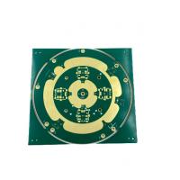
Multilayer PCB Fabrication, which is the creation of multi-level printed wiring boards, is a complex process that requires precision and expertise. Our experienced professionals specialize in multi-layer printed circuit board production and ensure that every step of the process is completed with the utmost care and attention to detail. Our multi-layer printed circuit board production services include a minimum line width of 0.1mm, copper thickness of 1-4oz, silkscreen colors of white, black, yellow, and more, board thickness of 0.2-3.2mm, and layer counts of 2-20. We are committed to providing the highest quality service and products to meet the specific needs of our customers.
| Parameter | Specification |
|---|---|
| Silkscreen Color | White, Black, Yellow, Etc. |
| Min. Line Width | 0.1mm |
| Layer Count | 2-20 |
| Min. Line Spacing | 0.1mm |
| Copper Thickness | 1-4oz |
| Surface Finish | HASL, ENIG, OSP, Immersion Silver, Immersion Tin, Etc. |
| Impedance Control | Yes |
| Board Thickness | 0.2-3.2mm |
| Solder Mask Color | Green, Blue, White, Black, Red, Etc. |
| Material | FR4, High TG FR4, Halogen Free, Rogers, Etc. |
JIETENG multi-layer PCB fabrication is a great solution for complex and intricate electronics designs. It is capable of producing multi-level printed circuit boards with various specs for a wide range of applications. The brand name, model number, place of origin, min. line width, silkscreen color, min. line spacing, copper thickness, and surface finish are all customizable.
Multi-layer PCB fabrication consists of multi-level printed circuit board assembly and multi-layer PCB assembly. The multi-level printed circuit board assembly provides high density interconnects, which can be used to build complex electronic devices. The multi-layer PCB assembly is used for assembling components on the printed circuit board. It involves assembling components, such as chips and resistors, onto the printed circuit board.
JIETENG multi-layer PCB fabrication is suitable for applications such as automotive, medical, industrial, and consumer electronics. It is also suitable for applications where fast and reliable signals are needed, such as communications, military, and aerospace. With its min. line width of 0.1mm, min. line spacing of 0.1mm, copper thickness ranging from 1-4oz, and surface finish options such as HASL, ENIG, OSP, Immersion Silver, and Immersion Tin, JIETENG multi-layer PCB fabrication ensures high quality and precise components for various applications.
Moreover, the silkscreen color can be customized according to customer needs, from white, black, yellow, to other colors. With its versatile features, JIETENG multi-layer PCB fabrication is the perfect solution for creating complex and precise electronic devices.
JIETENG's custom Multi-level Printed Circuit Board Fabrication service offers high-quality and reliable production for all types of Printed Circuit Boards. Our service is perfect for creating high-performance multi-level printed wiring boards with various materials, such as FR4, high TG FR4, Halogen Free, Rogers, and more. Our team of experienced engineers can help you choose the right material for your needs. We also offer impedance control for all of our products.
Our multi-level printed circuit board fabrication includes:
At JIETENG, we are committed to providing the best quality multi-level printed wiring board creation services. Contact us today for more information about our Multi-Level Printed Circuit Board Fabrication services.
We provide comprehensive support and service for Multilayer PCB Fabrication, including:
For more information, please contact our technical support team.
The packaging and shipping of Multilayer PCB Fabrication involves the following steps:


