|
|
[China]

Trade Verify
Address: Building 1, Huafeng Science and Technology Park, No. 54 Guangtian Road, Luotian County community, Songgang Town, Bao'an District, Shenzhen City
Contact name:Sales Manager

ShenZhen Jieteng Circuit Co., Ltd. |
|
Verified Suppliers
|
|
|
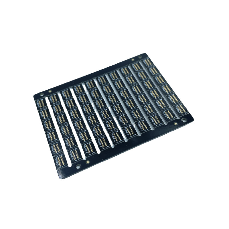
Factory direct sales of PCB medical equipment HDI blind hole board high-precision PCB processing
With Our Professional Departments, We Can Offer:
| Item | Specification | |
| 1 | Numbr of Layer | 1-80 Layers (standard) |
| 2 | Material | FR4, Aluminum, FPC |
| 3 | Surface Finish | HASL(LF), Gold plating, Enig,Immersion gold, Immersion Tin, OSP |
| 4 | Finish Board Thickness | 0.2mm-6.00 mm(8mil-126mil) |
| 5 | Copper Thickness | 1/2 oz min;12 oz max |
| 6 | Solder Mask | Green/Black/White/Red/Blue/Yellow |
| 7 | Min.Trace Width & Line Spacing | 0.075mm/0.1mm(3mil/4mil) |
| 8 | Min.Hole Diameter for CNC Driling | 0.1mm(4mil) |
| 9 | Min.Hole Diameter for punching | 0.9mm(35mil) |
| 10 | Biggest panel size | 610mm*508mm |
| 11 | Hole Positon | +/-0.075mm(3mil) CNC Driling |
| 12 | Conductor Width(W) | 0.05mm(2mil)or;+/-20% of original artwork |
| 13 | Hole Diameter(H) | PTH L:+/-0.075mm(3mil);Non-PTH L:+/-0.05mm(2mil) |
| 14 | Outline Tolerance | 0.125mm(5mil) CNC Routing;+/-0.15mm(6mil) by Punching |
| 15 | Warp & Twist | 0.70% |
| 16 | Insulation Resistance | 10Kohm-20Mohm |
| 17 | Conductivity | <50ohm |
| 18 | Test Voltage | 10-300V |
| 19 | Panel Size | 110×100mm(min);660×600mm(max) |
| 20 | Layer-layer misregistration | 4 layers:0.15mm(6mil)max;6 layers:0.25mm(10mil)max |
| 21 | Min.spacing between hole edge to circuity pattern of an inner layer | 0.25mm(10mil) |
| 22 | Min.spacing between board ouline to circuitry pattern of an inner layer | 0.25mm(10mil) |
| 23 | Board thickness tolerance | 4 layers:+/-0.13mm(5mil);6 layers:+/-0.15mm(6mil) |
| 24 | Impedance Control | +/-10% |
| 25 | Different Impendance | +-/10% |