
|
|
[China]

Trade Verify
Address: No. 26, Dongqing Street, High-tech Zone, Zhengzhou ,Henan, China
Contact name:Daniel

HENAN ZG INDUSTRIAL PRODUCTS CO.,LTD |
|
Verified Suppliers
|
|
|
Ge wafer to micro-electronics and opto-electronics industry in diameter range from 2 inch to 4 inch
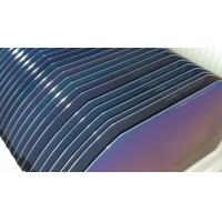
We are a worldwide supplier of single crystal Ge wafer ( Germanium wafer ) and single crystal Ge ingot , we have a strong advantage in providing Ge wafer to micro-electronics and opto-electronics industry in diameter range from 2 inch to 4 inch . Ge wafer is an elemental and popular semiconductor material , due to its excellent crystallographic properties and unique electric properties , Ge wafer is widly used in Sensor , Solar cell and Infrared optics applications . We can provide low dislocation and epi ready Ge wafers to meet your unique germanium needs . Ge wafer is produced as per SEMI. standard and packed in standard cassette with vacuum sealed in clean room enviroment , with a good quality control system , We are dedicated to providing clean and high quality Ge wafer products . We can offer both electronics grade and IR grade Ge wafer , please contact us for more Ge product information
Single Crystal Germanium Wafer Capability
SWI can offer both electronics grade and IR grade Ge wafer and Ge
ingot , please contact us for more Ge product information .
| Conductivity | Dopant | Resistivity ( ohm-cm ) | Wafer Size |
|---|---|---|---|
| NA | Undoped | >= 30 | Up to 4 inch |
| N type | Sb | 0.001 ~ 30 | Up to 4 inch |
| P type | Ga | 0.001 ~ 30 | Up to 4 inch |
Applications:
Semiconductor device , Microelectronics , Sensor , Solar cell , IR optics.
Ge Wafer Properties
| Chemical formula | Ge |
| Crystal structure | Cubic |
| Lattice parameter | a=0.565754 |
| Density ( g / cm3 ) | 5.323 |
| Thermal conductivity | 59.9 |
| Melting point ( °C ) | 937.4 |
Product Specification
| Growth | Czochralski |
|---|---|
| Diameter | Ø 2" / Ø 3" / Ø 4" |
| Thickness | 500 um ~ 625 um |
| Orientation | <100> / <111> / <110> or others |
| Conductivity | P - type / N - type |
| Dopant | Gallium / Antimony / Undoped |
| Resistivity | 0.001 ~ 30 ohm-cm |
| Surface | SSP / DSP |
| TTV | <= 10 um |
| Bow / Warp | <= 40 um |
| Grade | Electronics grade |


