
|
|
[China]

Trade Verify
Address: Shenzhen Omini Technology Co., Ltd 605, Tongxin Technology Building, Qiaotou Community, Fuhai Street, Baoan District, Shenzhen
Contact name:Xu

Shenzhen Omini Technology Co.,Ltd |
|
Verified Suppliers
|

|
|
TV Motherboard Multilayer Printed Wire Board PCB Control Board
Quick details:
Base Material: Shengyi S1000-2M
Copper Thickness: 2 oz
Board Thickness: 2.0 mm
Min. Hole Size: 0.2mm
Min. Line Width: 4 mil
Min. Line Spacing: 4 mil
Surface Finishing: HASL
Board Size: Customize
Application:Computer Demand
IPC Degree: IPC Class 2
Maximum board width: Customize
Type: Multilayer PCB
Certificate: TS16949.ISO14001.ROHS. ISO9001
Color: Green
Package: Vacuum packing
Description of TV Motherboard Multilayer PCB
A TV motherboard is the main circuit board that controls the functions of a television set. It typically consists of a multilayer printed circuit board (PCB) that contains various electronic components, such as microcontrollers, memory chips, power regulators, and connectors. The multilayer PCB is designed to accommodate the complex network of connections required for these components to communicate with each other.
In older electronic devices, the power supply, video processing, and display driver sections of a TV were often located on separate PCBs that were connected via various connectors and wiring. However, modern LED TVs have all of these components integrated onto a single PCB, which simplifies installation and repair processes by requiring only one point of connection and reducing the need for complex wiring and harnesses. This design offers improved ease of use and maintenance for the end user.
Process of TV Motherboard Multilayer PCB
The manufacturing process of multilayer PCBs involves several steps that can be summarized as follows. Firstly, the desired design is developed and encoded to ensure error-free performance. Next, the design is printed, and copper is utilized to build the inner layers of the PCB. Unwanted copper is then removed, and the layers are fused through lamination. Drilling is done after locating the drill spot with an x-ray machine, and the layers are plated with a chemical to fuse them together. The outer layer is imaged and plated, and final etching is done to establish the PCB connections. Solder mask is applied, and silk-screening is done to mark important information on the PCB. The PCB is then electrically tested for reliability before it is profiled and cut according to customer requirements. Finally, the board is inspected for errors and sent for delivery.
Specification of Omini Multi - layer Printed Circuit Board
| Layer | 2-24 layer |
| Material | FR-4 Standard Tg 150℃, FR4-HighTg170℃, FR4- High Tg180℃, FR4- Halogen- free, FR4- Halogen- Free&High-Tg |
| Board thickness | 0.4mm-5.0mm |
| Board side | Min 6*6mm Max 600*700mm |
| Min.drilled hole size | 0.25mm |
| Min.line width | 0.075mm(3mil) |
| Min.line spaceing | 0.075mm(3mil) |
| Surface finish/treatment | Electroless/immersion gold/ENIG/Immersion silver/Organic solderability |
| Copper thickness | 0.5 oz - 2.0oz |
| Solder mask color | green/black/white/red/blue/yellow |
| Inner packing | Vacuum packing, Plastic bag |
| Outer packing | Standard carton packing |
| Hole tolerance | PTH:±0.076, NTPH:±0.05 |
| Certificate | UL, ISO9001, ISO14001, RoHS, CQC |
| Profiling Punching | Routing, V-CUT, Beveling |
| Assembly Service | Providing OEM service to all sorts of printed circuit board assembly |


FAQ:
Q1:Does Omini have enough capacity to prodece high-quality products?
A: Omini has 20 years of history in manufacturing PCB, more than 200 employees and 10,000㎡ factory area.We got the UL, ISO9001 certificates, and our production is sold abroad. We have engouh machines & equipment to ensure the quality, please check our Production Equipment list picturers.
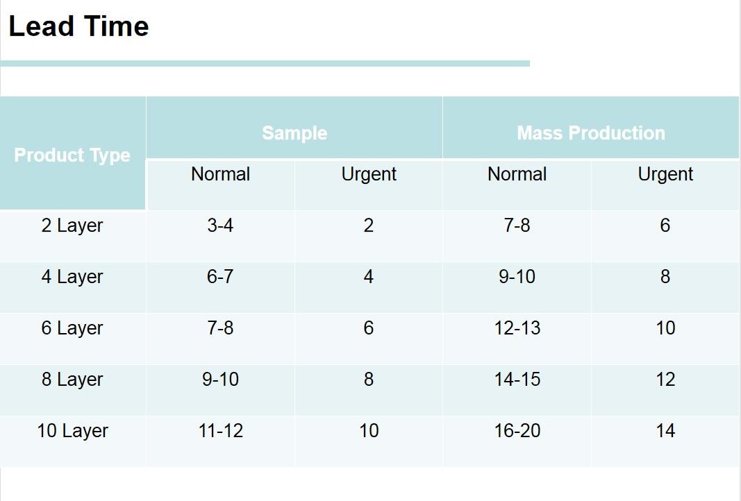
Q2:How long does customers need to wait for the quotation and lead time?
A: We have a prefessional group to deal with your inquiry. In our working time, we will reply to your email within 30 minutes to show we have received your inquiry, Then we will send you our quotation in no more than 6 hours. Please noticed our working time is Monday to Friday, 8am to 24pm.
Q3:How can I make sure my PCB gerber is safety?
A: We promise we won't divulge your gerber to the 3rd party, one of our responsibilities is protecting customer information privacy and security, customer information can be included: company name, address, number, trademark, ect. And we could sign NDA with client if necessary.


