
|
|
[China]

Trade Verify
Address: Rm5-616,No.851,Dianshanhu avenue, Qingpu area,Shanghai city,CHINA
Contact name:Wang

SHANGHAI FAMOUS TRADE CO.,LTD |
|
Verified Suppliers
|

|
|
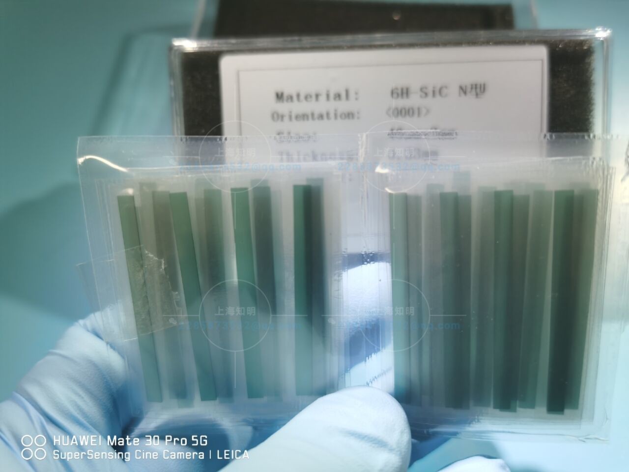
4inch dia100m 4H-N type Production grade DUMMY grade SiC substrates,Silicon Carbide substrates for semiconductor device,
4h-semi 4h-N customized square shape sic wafers
Application areas
1 high frequency and high power electronic devices Schottky diodes,
JFET, BJT, PiN, diodes, IGBT, MOSFET
2 optoelectronic devices: mainly used in GaN/SiC blue LED substrate material (GaN/SiC) LED
Advantagement
• Low lattice mismatch
• High thermal conductivity
• Low power consumption
• Excellent transient characteristics
• High band gap
Silicon Carbide SiC crystal substrate wafer carborundum
SILICON CARBIDE MATERIAL PROPERTIES
| Product Name: | Silicon carbide (SiC) crystal substrate | ||||||||||||||||||||||||
| Product Description: | 2-6inch | ||||||||||||||||||||||||
| Technical parameters: |
| ||||||||||||||||||||||||
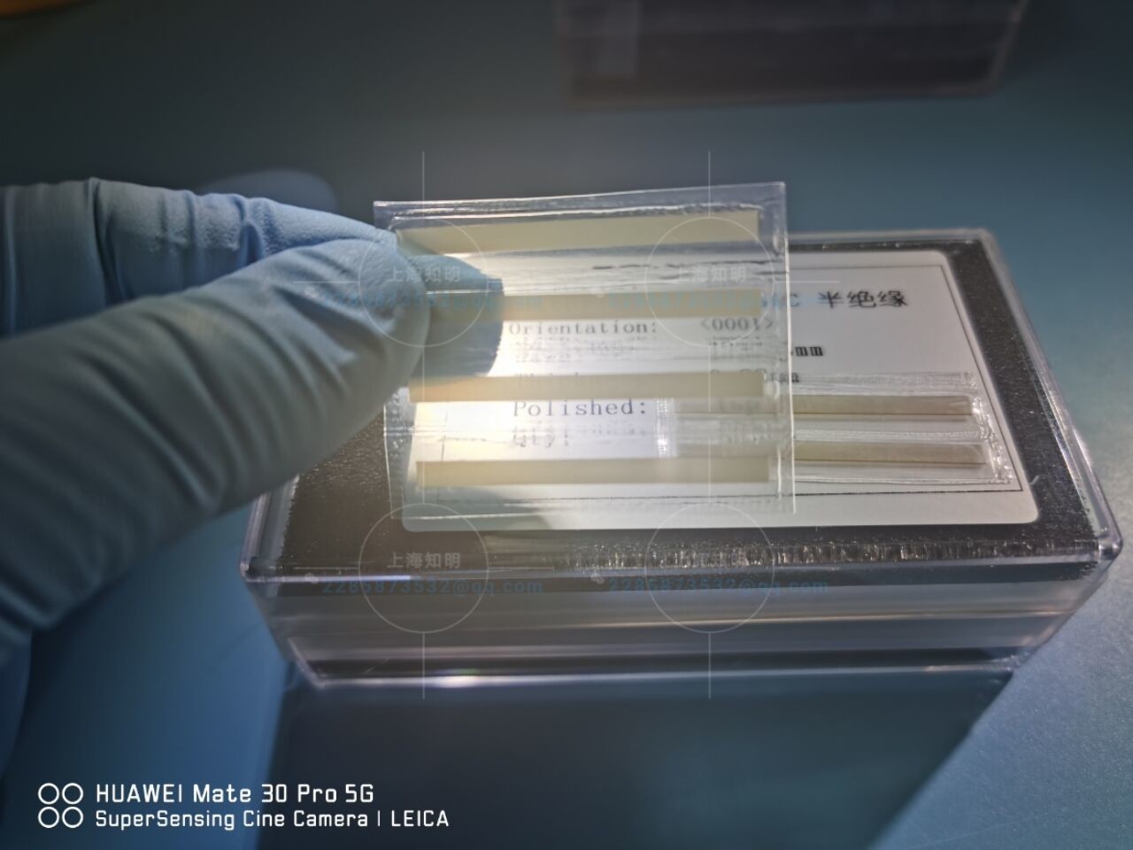
| Specifications: | 6H N-type 4H N-type semi-insulating dia2 "x0.33mm, dia2" x0.43mm,dia2''x1mmt, 10x10mm, 10x5mm Single throw or double throw, Ra <10A | ||||||||||||||||||||||||
| Standard Packaging: | 1000 clean room, 100 clean bag or single box packaging |
2. substrates size of standard
4 inch diameter Silicon Carbide (SiC) Substrate Specification | |||||||||
| Grade | Zero MPD Grade | Production Grade | Research Grade | Dummy Grade | |||||
| Diameter | 100.0 mm±0.5 mm | ||||||||
| Thickness | 350 μm±25μm (200-500um thickness also is ok) | ||||||||
| Wafer Orientation | Off axis : 4.0° toward <1120> ±0.5° for 4H-N/4H-SI On axis : <0001>±0.5° for 6H-N/6H-SI/4H-N/4H-SI | ||||||||
| Micropipe Density | ≤1 cm-2 | ≤5 cm-2 | ≤15 cm-2 | ≤50 cm-2 | |||||
| Resistivity | 4H-N | 0.015~0.028 Ω•cm | |||||||
| 6H-N | 0.02~0.1 Ω•cm | ||||||||
| 4/6H-SI | ≥1E5 Ω·cm | ||||||||
| Primary Flat and length | {10-10}±5.0° ,32.5 mm±2.0 mm | ||||||||
| Secondary Flat Length | 18.0mm±2.0 mm | ||||||||
| Secondary Flat Orientation | Silicon face up: 90° CW. from Prime flat ±5.0° | ||||||||
| Edge exclusion | 3 mm | ||||||||
| TTV/Bow /Warp | ≤15μm /≤25μm /≤40μm | ||||||||
| Roughness | Polish Ra≤1 nm ,CMP Ra≤0.5 nm | ||||||||
| Cracks by high intensity light | None | 1 allowed, ≤2 mm | Cumulative length ≤ 10mm, single length≤2mm | ||||||
| Hex Plates by high intensity light | Cumulative area ≤1% | Cumulative area ≤1% | Cumulative area ≤3% | ||||||
| Polytype Areas by high intensity light | None | Cumulative area ≤2% | Cumulative area ≤5% | ||||||
| Scratches by high intensity light | 3 scratches to 1×wafer diameter cumulative length | 5 scratches to 1×wafer diameter cumulative length | 5 scratches to 1×wafer diameter cumulative length | ||||||
| edge chip | None | 3 allowed, ≤0.5 mm each | 5 allowed, ≤1 mm each | ||||||
| Contamination by high intensity light | None | ||||||||
Sic wafer & ingots 2-6inch and other customized size also can be provided.
3.Pictures of delivery Products before


A:semiconductor wafers and Optical lens,mirrors,windows,filters,prisms
A: In general delivery time is about one month for custom produced optics.except stock ones or some special optics.
A: We can provide free samples if we have stock optics as your request,while custom produced samples are not free.
MOQ is 10pcs for most of wafer or lens , while MOQ could be only one piece if you need a element in big dimention.
T/T,L/C,VISA,Paypal,Alipay or Negotiation.


