Home Companies SHANGHAI FAMOUS TRADE CO.,LTD

customized Thickness 1.5mm 4" 4H-N sic Crystal as-cut blank Wafers

SHANGHAI FAMOUS TRADE CO.,LTD

Contact Us

[China] country

Trade Verify

Address: Rm5-616,No.851,Dianshanhu avenue, Qingpu area,Shanghai city,CHINA

Contact name:Wang

Inquir Now

SHANGHAI FAMOUS TRADE CO.,LTD

Verified Suppliers
  • Trust
    Seal
  • Verified
    Supplier
  • Credit
    Check
  • Capability
    Assessment

customized Thickness 1.5mm 4" 4H-N sic Crystal as-cut blank Wafers

Country/Region china
City & Province shanghai shanghai
Categories Other Metals & Metal Products
InquireNow

Product Details

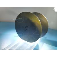
4inch dia100m 4H-N type Production grade DUMMY grade SiC substrates,Silicon Carbide substrates for semiconductor device,

customized thickness 4inch 4H-N silicon carbide crystal sic wafers  for 4inch seed crystal grade;


Silicon Carbide SiC crystal substrate wafer carborundum

SILICON CARBIDE MATERIAL PROPERTIES

Product Name:Silicon carbide (SiC) crystal substrate
Product Description:2-6inch 
Technical parameters:
Cell structureHexagonal
Lattice constanta = 3.08 Å c = 15.08 Å
PrioritiesABCACB (6H)
Growth methodMOCVD
DirectionGrowth axis or Partial (0001) 3.5 °
PolishingSi surface polishing
Bandgap2.93 eV (indirect)
Conductivity typeN or seimi ,high purity
Resistivity0.076 ohm-cm
Permittivitye (11) = e (22) = 9.66 e (33) = 10.33
Thermal conductivity @ 300K5 W / cm. K
Hardness9.2 Mohs
Specifications:6H N-type 4H N-type semi-insulating dia2 "x0.33mm, dia2" x0.43mm,dia2''x1mmt, 10x10mm, 10x5mm Single throw or double throw, Ra <10A
Standard Packaging:1000 clean room, 100 clean bag or single box packaging


Application of silicon carbide in power device industry
 
Compared with silicon (Si) devices, silicon carbide (SiC) power devices can effectively achieve high efficiency, miniaturization and light weight of power electronic systems. The energy loss of silicon carbide power devices is only 50% of that of Si devices, the heat generation is only 50% of that of silicon devices, and it has a higher current density. At the same power level, the volume of silicon carbide power modules is significantly smaller than that of silicon power modules. Taking the intelligent power module IPM as an example, using silicon carbide power devices, the module volume can be reduced to 1/3 to 2/3 of silicon power modules.
 
There are 3 types of silicon carbide power diodes: Schottky diodes (SBD), PIN diodes and junction barrier control Schottky diodes (JBS). Due to the Schottky barrier, SBD has a lower junction barrier height, so SBD has the advantage of low forward voltage. The emergence of silicon carbide SBD increased the application range of SBD from 250V to 1200V. At the same time, its high temperature characteristics are good, from room temperature to 175°C limited by the shell, the reverse leakage current hardly increases. In the application field of rectifiers above 3kV, silicon carbide PiN and silicon carbide JBS diodes have attracted attention due to their higher breakdown voltage, faster switching speed, smaller volume and lighter weight than silicon rectifiers.
 
Silicon carbide power MOSFET devices have ideal gate resistance, high-speed switching performance, low on-resistance and high stability. It is the preferred device in the field of power devices below 300V. It is reported that a silicon carbide MOSFET with a blocking voltage of 10kV has been successfully developed. Researchers believe that silicon carbide MOSFET will occupy an advantageous position in the field of 3kV to 5kV.
 
Silicon carbide insulated gate bipolar transistors (SiC BJT, SiC IGBT) and silicon carbide thyristors (SiC Thyristor), silicon carbide P-type IGBT devices with a blocking voltage of 12kV have good forward current capability. The on-resistance of silicon carbide IGBT devices can be compared with unipolar silicon carbide power devices. Compared with Si bipolar transistors, SiC bipolar transistors have 20-50 times lower switching losses and lower conduction voltage drop. Silicon carbide BJT is mainly divided into epitaxial emitter and ion implanted emitter BJT, and the typical current gain is between 10-50.
 
   
Performance Unit Silicon Si  Silicon Carbide SiC    Gallium Nitride GaN
Band gap eV            1.12            3.26                             3.41
Breakdown electric field MV/cm 0.23 2.2 3.3
Electron mobility cm^2/Vs 1400 950 1500
Drift speed 10^7 cm/s 1 2.7 2.5
Thermal conductivity W/cmK 1.5 3.8 1.3
 

2. substrates size of standard

4 inch diameter Silicon Carbide (SiC) Substrate Specification

GradeZero MPD GradeProduction GradeResearch GradeDummy Grade
Diameter100.0 mm±0.5 mm
Thickness350 μm±25μm (200-2000um thickness also is ok)
Wafer OrientationOff axis : 4.0° toward <1120> ±0.5° for 4H-N 
Micropipe Density≤1 cm-2≤5 cm-2≤15 cm-2≤50 cm-2
Resistivity4H-N0.015~0.028 Ω•cm
6H-N0.02~0.1 Ω•cm
4/6H-SI≥1E5 Ω·cm
Primary Flat and length{10-10}±5.0° ,32.5 mm±2.0 mm
Secondary Flat Length18.0mm±2.0 mm
Secondary Flat OrientationSilicon face up: 90° CW. from Prime flat ±5.0°
Edge exclusion3 mm
TTV/Bow /Warp≤15μm /≤25μm /≤40μm
RoughnessPolish Ra≤1 nm ,CMP Ra≤0.5 nm
Cracks by high intensity lightNone1 allowed, ≤2 mmCumulative length ≤ 10mm, single length≤2mm
Hex Plates by high intensity lightCumulative area ≤1%Cumulative area ≤1%Cumulative area ≤3%
Polytype Areas by high intensity lightNoneCumulative area ≤2%Cumulative area ≤5%
Scratches by high intensity light3 scratches to 1×wafer diameter cumulative length5 scratches to 1×wafer diameter cumulative length5 scratches to 1×wafer diameter cumulative length
edge chipNone3 allowed, ≤0.5 mm each5 allowed, ≤1 mm each
Contamination by high intensity lightNone

Sic wafer & ingots  2-6inch and other customized size   also can be provided.


3.Products detail display


Delivery & Package

FAQ

Q1. Is your company a factory or trade company?


We are the factory and we also can do export ourself.


Q2.Is you company only work with sic  business?

yes; however we don‘t grow the sic crystal by self. 


Q3. Could you supply sample?

Yes,we can supply sapphire sample according to customer's requirement.


Q4. Do you have any stock of sic wafers ?

we usually keep some standard size sic wafers from 2-6inch wafers  in stock.


Q5.Where is your company located?


Our company located in shanghai ,China.


Q6. How long will take to get the products?

Generally it will take 3~4 weeks to process.It is depend on the quantity and the size of the  products.


Hot Products

Sapphire Crystal Cr3+Doped Ruby Cr Al2O3 Crystal Substrate Ruby Wafer Polishing Specification for ...
0.3mm/0.4mm/0.5mm sapphire window thin glass wafers for semiconductor or electron Optical Windows ...
Sapphire Washers Wafer Bearings Windows Rods Tubes Ruby Glass The identification method of sapphire ...
Sapphire windows sapphire glass crystal sapphire optical glass window ar coating Sapphire Windows ...
6 inch synthetic sapphire Bf33 0.725mm Wafer for GaAs Features for 6 in Sapphire Wafer Single or ...
Product Description: Single crystal sapphire is widely used due to its excellent optical, thermal ...