
|
|
[China]

Trade Verify
Address: Rm5-616,No.851,Dianshanhu avenue, Qingpu area,Shanghai city,CHINA
Contact name:Wang

SHANGHAI FAMOUS TRADE CO.,LTD |
|
Verified Suppliers
|
|
|
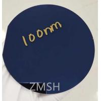
2” 3’’ FZ SiO2 Single Crystal IC Chips 100um 200um Dry Wet Oxidation Layer 100nm 300nm
Product description:
The silicon wafer is formed through a furnace tube in the presence of an oxidizing agent at an elevated temperature, a process called thermal oxidation A layer of silica. The temperature range is controlled from 900 to 1,250℃; The ratio of the oxidizing gas H2:O2 is between 1.5:1 and 3:1. In accordance with the According to the size of the silicon wafer does not oxidize the thickness will have different flow does not consume. The substrate silicon wafer is 6 "or 8" monocrystalline silicon with an oxide layer thickness of 0.1μm to 25μm.The thickness of the oxide layer of the general silicon wafer is mainly concentrated below 3μm, which can be stable at present Quantitative production of high quality thick oxide layer (3μm or more) silicon wafer countries and regions or the United States.
Features:
Silicon material is hard and brittle (Mohs 7.0); Band gap width 1.12eV; The absorption of light is in the infrared band, with high emissivity and refractive index (3.42); Silicon has obvious thermal conductivity and thermal expansion properties (linear expansion coefficient 2.6*10^-6/K), silicon melting volume shrinks, solidification expansion, has a large surface tension coefficient (surface tension 720 dyn/cm); At room temperature, silicon is not malleable, and the temperature is higher than 800 degrees. It is obviously shaped, and it is prone to plastic deformation under the action of stress. The tensile strength of silicon is greater than the anti-reducing stress, and it is easy to produce bending and warping during processing.
Technical Parameters:
| Items | Parameters |
| Density | 2.3g/cm3 |
| Melting point | 1750℃ |
| Boiling point | 2300℃ |
| Refractive index | 1.4458±0.0001 |
| Mol. wt | 60.090 |
| Appearance | grey |
| Solubility | Insoluble |
| Sinter point | 900℃~1500℃ |
| Preparation method | dry/wet oxidation |
| Warp | 8um |
| Bow | 8um |
| TTV | 8um |
| Orientation | 110 |
| Ra | 0.4nm |
| Application | 5G |
Applications:
Monocrystalline silicon can be used for diode level, rectifier device level, circuit level and solar cell level monocrystalline product production and deep processing manufacturing, its follow-up products integrated circuit and semiconductor separation devices have been widely used in various fields, and also occupies an important position in military electronic equipment. Today, with the rapid development of photovoltaic technology and micro-semiconductor inverter technology, solar cells produced by silicon single crystals can directly convert solar energy into light energy, realizing the beginning of the green energy revolution. The Beijing Olympic Games show the concept of "Green Olympics" to the world, and the use of monocrystalline silicon is a very important part of it.

Other product:

FAQ:
Q: What is the Brand Name of SiO2 Single Crystal?
A: The Brand Name of SiO2 Single Crystal is ZMSH.
Q: What is the Certification of SiO2 Single Crystal?
A: The Certification of SiO2 Single Crystal is ROHS.
Q: Where is the Place of Origin of SiO2 Single Crystal?
A: The Place of Origin of SiO2 Single Crystal is CHINA.
Q: What is the MOQ of SiO2 Single Crystal at one time?
A: The MOQ of SiO2 Single Crystal is 25pcs at one time.


